The moment you wake a smartphone screen, millions of pixels light up at their own assigned brightness, all at once. Who tells each individual pixel "shine exactly this much, right now"? The circuit layer that does this job is hidden behind the screen — it is called the backplane.
This is the first article in the series "Display Backplane Processes." We will walk through the manufacturing steps that create millions of invisible transistors on a sheet of glass, following the same order a real fab does, starting from fundamentals. Everything here stays at a level anyone can verify in public sources — textbooks, papers, patents, encyclopedias — and each article ends with its actual references.
Look closely at a screen
Have you ever looked at a screen from very close up? A magnifier, or even a single drop of water, reveals what it really is — the surface that looked seamless is in fact a dense lattice of small emitting elements in red, green and blue, called sub-pixels.
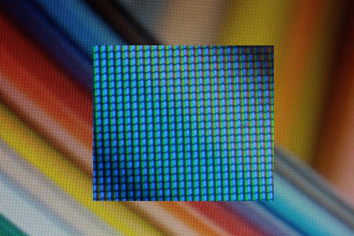
The sub-pixel lattice revealed under magnification. Photo: Wikimedia Commons (Politelyinsulting, CC BY-SA 3.0)
A common FHD resolution (1920×1080) already contains about 2.07 million pixels, or about 6.22 million sub-pixels. Each of those millions of emitting elements changes its brightness independently, tens to hundreds of times per second. That means every sub-pixel needs at least one switch of its own.
The difficulty, in numbers
"Millions" is hard to feel. Working out the actual numbers by resolution makes it clear what kind of problem a backplane is. Sub-pixel count is width × height × 3 (RGB), and the time allotted to one row is 1 ÷ (refresh rate × number of rows), because the panel is scanned one row at a time from top to bottom within each frame.
| Resolution | Pixels | Sub-pixels (= minimum TFT count) | Time per row at 120 Hz |
|---|---|---|---|
| HD 1366×768 | ~1.05 million | ~3.15 million | 10.85 µs |
| FHD 1920×1080 | ~2.07 million | ~6.22 million | 7.72 µs |
| QHD+ 3200×1440 | ~4.61 million | ~13.82 million | 5.79 µs |
| 4K UHD 3840×2160 | ~8.29 million | ~24.88 million | 3.86 µs |
| 8K UHD 7680×4320 | ~33.18 million | ~99.53 million | 1.93 µs |
A single 4K panel holds 24.88 million transistors; at 8K the figure approaches one hundred million. And the time allowed to fill one row is a little under four microseconds. Within four millionths of a second, every pixel in that row must be charged to its target voltage so the scan can move on.
A simple calculation shows why this timing constraint dictates the choice of material. If we take the storage capacitance of one pixel as 0.5 pF and the required voltage swing as 5 V, the charging current is I = C × ΔV ÷ t = 0.5 pF × 5 V ÷ 3.86 µs ≈ 0.65 µA. The number itself looks small, but the difficulty is that this current must be delivered by a single transistor a few tens of micrometres across — and by all 24.88 million of them identically. In a material where electrons move poorly, charging does not finish in time, and that pixel comes out darker than intended.
A screen is two planes
Cut a display panel in cross-section and you see two main parts. The upper part actually produces light — the frontplane: an organic emitting stack in an OLED, liquid crystal and colour filters in an LCD. The lower part is the subject of this series, the backplane: a vast array of switches attached to each of those sub-pixels, that is, thin-film transistors (TFTs). On top sit the touch layer that reads fingertip position and the cover window that protects the screen.
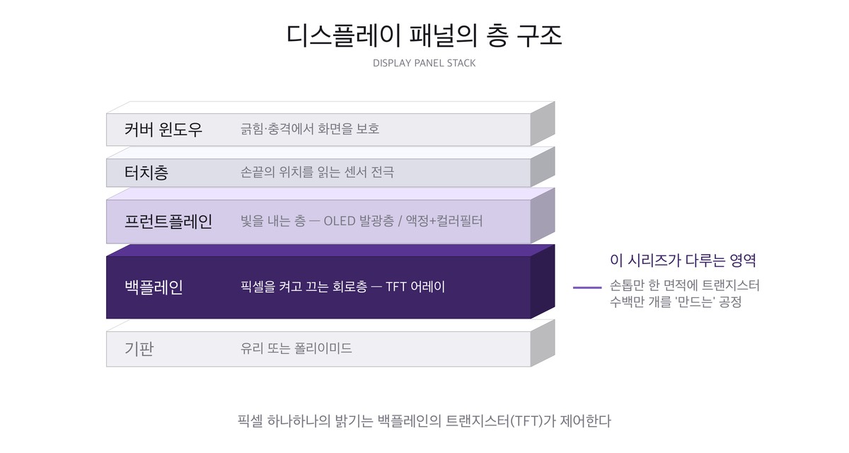
- Frontplane — makes light. The "face" of the screen.
- Backplane — switches pixels on and off. The "brain and hands" of the screen.
- However good the emitting material, an imprecise backplane yields a blotchy image.
This is also where the name "thin film" comes from. Unlike the transistors in a semiconductor chip, which are carved out of a thick silicon wafer, display transistors are built by stacking films tens to hundreds of nanometres thick on top of glass. A wafer is a 30 cm disc; a display glass substrate is a giant plate two to three metres on a side. "Over an enormous area, extremely thin, millions of them identical" — that is the intrinsic difficulty of backplane manufacturing.
The invention of active-matrix driving — a lineage
The idea of a backplane did not appear overnight. The lineage documented in public literature runs more than sixty years.
The thin-film transistor as a device was first set out in a journal in 1962 (P. K. Weimer, "The TFT — A New Thin-Film Transistor"). The proposition that you could deposit a semiconducting film on an insulating substrate instead of carving a wafer is the direct ancestor of today's backplane.
Attaching that device to a screen came in 1973. A 6×6 inch liquid-crystal panel at 20 lines per inch was reported driven by a TFT array (T. P. Brody et al.), and this is the starting point of what we now call active-matrix driving. "Active" means each pixel owns its switch and storage capacitor, and therefore holds its own state until its turn comes round again. In passive driving, with no switch per pixel, the time each pixel is illuminated shrinks as the number of rows grows, and brightness and contrast collapse. This is exactly why the "time per row" column above matters.
The next question was what to build it from. In 1979 a field-effect device made from amorphous silicon was reported (P. G. Le Comber, W. E. Spear et al.), opening the way to spraying cheap transistors across large-area glass — and with it, the LCD era. In 1986, a method of flash-crystallising amorphous silicon with an excimer laser to make polycrystalline silicon TFTs was reported (T. Sameshima et al.), opening the door to LTPS. And in 2004, transparent TFTs made at room temperature on a flexible substrate from an amorphous oxide semiconductor were reported (K. Nomura, H. Hosono et al.), beginning the oxide backplane lineage.
The device of 1962, the driving scheme of 1973, and the three channel materials of 1979, 1986 and 2004 — every screen we use today stands on these five events.
Why the backplane decides image quality
OLED in particular is a current-driven device. The current pushed into a pixel is its brightness, so the slightest wobble in a transistor's current-supplying ability shows up directly as brightness non-uniformity, known in the industry as mura. In the LCD era the transistor was close to a simple on/off switch applying a voltage to liquid crystal; in an OLED the transistor must also act as an analogue current source. The requirement is of a completely different order.
The nature of the error changes too. For a switch, only "open or closed" needs to be right, so device-to-device variation barely reaches the screen. A current source, however, delivers a different current if its threshold voltage shifts by as little as 0.1 V, and that becomes a visible brightness difference. The human eye is especially sensitive to gentle brightness gradients across a wide area, so even a few percent of spread reads as a stain. For an OLED backplane, therefore, the uniformity of tens of millions of devices matters more than the performance of any one of them.
Market demands pile on top. Higher resolution makes pixels smaller; a 120 Hz refresh rate shortens switching time; saving battery requires leakage current to be extremely small. In the end, the ability to build smaller, faster, more uniform, less leaky transistors on glass is the whole of backplane technology.
Three generations of backplane — the fork in materials
Backplane material technology has developed along three broad branches. All are industry-standard technologies documented in public literature, and the mobility figures below are representative values reported in an academic review ("Excimer-laser annealing for low-temperature poly-Si TFTs," J. Inf. Disp. 4(1) (2003)).
- a-Si (amorphous silicon) — the oldest approach, established alongside LCDs from the 1980s. It is cheap and easy to deposit over large areas at low temperature, but the disordered atomic arrangement makes it hard for electrons to travel (electron mobility around 0.5–1 cm²/Vs). It remains entirely adequate for large TV- and monitor-class LCDs.
- LTPS (low-temperature polycrystalline silicon) — amorphous silicon melted for an instant by a laser and refrozen as crystal. Electron mobility jumps to around 100 cm²/Vs, roughly a hundredfold over a-Si, which allows fast driving circuitry to fit inside a small pixel. The "low temperature" qualifier means crystallisation is achieved below the temperature at which glass deforms (roughly 600 °C). It is the de facto standard for smartphone OLED.
- Oxide (IGZO family) — a semiconductor made from indium, gallium and zinc oxide. Its mobility of about 10 cm²/Vs is lower than LTPS but more than ten times higher than a-Si, and above all its leakage current is extraordinarily small, so a still image holds even when driving pauses. It is expanding into tablets, notebooks and large OLED.
Putting the three side by side makes the logic of the choice visible.
| Item | a-Si | LTPS | Oxide (IGZO family) | LTPO |
|---|---|---|---|---|
| Channel structure | Amorphous silicon | Polycrystalline silicon | Amorphous oxide | Both channels present |
| Electron mobility (cm²/Vs) | ~0.5–1 | ~100 | ~10 | Either, by region |
| First reported | 1979 | 1986 (ELA) | 2004 | Commercial in the 2010s |
| Uniformity | Good — disorder is at least even | Wide spread from grain boundaries | Good | Corrected by mixed design |
| Leakage current | Moderate | Large | Very small | Oxide handles the hold phase |
| Peak process temperature | ~300 °C class | Below ~600 °C, plus laser | Room temperature to ~350 °C | Follows the LTPS budget |
| Number of process steps | Fewest | Most | Intermediate | More than LTPS |
| Main application | Large LCD | Smartphone OLED | Tablet, notebook, large OLED | Variable-refresh phones and watches |
What deserves attention is that no single material wins every row. LTPS dominates on mobility but loses on uniformity and leakage, and needs the most process steps. Oxide is good on leakage and uniformity but lacks the mobility to fit a large circuit inside a pixel. a-Si is cheap but cannot serve as an OLED current source.
Hence the arrival of the LTPO (LTPS + Oxide) hybrid in recent smartphones, mixing both inside one pixel — LTPS where fast switching is needed, oxide where nothing may leak — which enables variable-refresh screens that drop to 1 Hz to save battery. As the last column shows, LTPO is not a new material but an arrangement in which each fills the other's empty cells. We are in an era where the choice of backplane material determines the character of the product.
This series walks through the manufacturing process of the LTPS backplane, which has the most steps and the most to teach. Understand LTPS and the a-Si and oxide flows follow naturally as subsets or variants of it.
Why the glass keeps getting bigger
No backplane discussion escapes the topic of substrate generations. Moving up a generation means the sheet of glass processed at one time gets larger. The dimensions below are the values a patent specification lists as industry practice (US 8,093,136). Areas and ratios are calculated directly from those dimensions.
| Generation | Glass size (mm) | Area (m²) | Relative to Gen 3 |
|---|---|---|---|
| Gen 3 | 550 × 650 | 0.36 | 1.0× |
| Gen 4 | 730 × 920 | 0.67 | 1.9× |
| Gen 5 | 1100 × 1300 | 1.43 | 4.0× |
| Gen 6 | 1500 × 1850 | 2.78 | 7.8× |
| Gen 7 | 1870 × 2200 | 4.11 | 11.5× |
| Gen 8 | 2200 × 2400 | 5.28 | 14.8× |
| Gen 10 | 2950 × 3400 | 10.03 | 28.1× |
The reason for moving up is simple. The time a piece of process equipment needs for one sheet does not scale in proportion to area, so the more panels you cut from one big sheet, the lower the cost per panel. The same patent notes that a 2200 × 2500 mm substrate can be singulated into six 55-inch panels, and direct arithmetic confirms it — a 55-inch 16:9 panel is about 1218 × 685 mm, so 2500 ÷ 1218 = 2 and 2200 ÷ 685 = 3, giving six.
That calculation, however, is an upper bound that ignores edge exclusion and scribe allowance. On a real line a strip around the rim of the glass is unusable and the cut lines between panels need clearance, so the practical count is often lower. Choosing a generation is ultimately a question of how neatly the intended panel size tiles into the glass dimensions. A poor fit wastes area, and a bigger sheet can end up costing more.
This sheer size is what sets the difficulty of the process. If one Gen 8 sheet yields six 4K panels, the transistors that must be built on that single sheet number about 149.3 million (24.88 million × 6). Even if the probability of any one device failing were only one in a million (1 ppm), each panel would carry roughly 25 defective devices on average. Twenty-five dots in the middle of a screen means a reject. This is why backplane manufacturing is called an industry of yield, and why this series devotes three whole articles (18–20) to cleaning alone.
Three common misconceptions
- "Higher mobility is always better." Mobility only says how well current flows. What actually matters in an OLED pixel is how alike tens of millions of devices are, and high-mobility LTPS in fact shows a wider device-to-device spread because of grain boundaries. That is why pixel circuits add several compensation transistors to cancel the spread.
- "The backplane is back-end plumbing, unrelated to image quality." If the emitting material sets colour and efficiency, the backplane sets how much of that potential is actually extracted. Image sticking, mura, crushed low-luminance greyscale and the achievable range of variable refresh are all backplane problems.
- "One transistor per pixel." An LCD generally needs one, but an OLED pixel circuit consists of several transistors and capacitors for compensation. That is why the table above labels the sub-pixel count as the minimum TFT count; the real device count is several times higher.
The map of this series — 9 stages, 20 articles
From the moment a glass substrate enters the fab until it emerges as a finished backplane, it passes through nine broad stages. This map is the table of contents for the whole series.
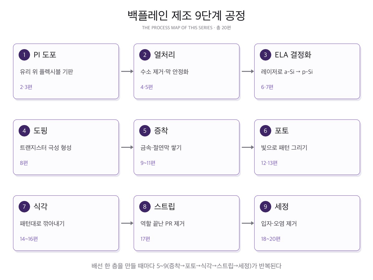
- PI coating (articles 2–3) — the secret of the folding screen. Polyimide is spread on glass to create a flexible substrate.
- Heat treatment (4–5) — a warm-up that drives hydrogen out of the film in advance. Skip it and the film bursts in the next step.
- ELA crystallisation (6–7) — the heart of LTPS: an excimer laser melts amorphous silicon for an instant and turns it polycrystalline.
- Doping (8) — impurities are implanted into silicon to inscribe transistor polarity (N-type, P-type).
- Deposition (9–11) — the stage of vacuum and plasma. Metal wiring and insulating films are stacked one layer at a time.
- Photolithography (12–13) — photoresist and ultraviolet light draw the circuit pattern "as if photographing" it.
- Etching (14–16) — shared concepts and parameters, then dry etching, then wet etching. The art of carving to pattern, and the fight against corrosion.
- Stripping (17) — the photoresist, its job done, is cleanly removed.
- Cleaning (18–20) — invisible particles decide yield. Why particles stick, and how to take them off.
One thing to say in advance: stages 5 through 9 (deposition → photo → etch → strip → clean) are not a single lap. The cycle repeats for every wiring layer built, and a single backplane sends this wheel around many times — because the transistor gate, the source/drain, and the pixel electrode are each a separate layer.
That repetition is the substance behind the "number of process steps" row in the table above. Changing the material really means changing how many extra laps the wheel must run, and each lap brings one more mask, several more tools, and one more inspection. LTPS is expensive not because of material cost but because of lap count.
Beginning the series
Every article follows the same three-part structure. Principle (why this process is needed) → Equipment (what does it) → Control points (what the floor watches). Bridging textbook principle and shop-floor instinct within a single article is the aim of this series. All content stays at the level of public literature, no specific company, product or production line is discussed, and the sources for anything cited are listed at the end of each article.
The next article starts with the first process — PI (polyimide) coating, the thing that made folding screens possible. It is the story of spreading a liquid on glass and thereby "making" a substrate.
References
- P. K. Weimer, "The TFT — A New Thin-Film Transistor," Proceedings of the IRE 50(6), 1462 (1962) : the original statement of the thin-film transistor concept — a transistor made from deposited films on an insulating substrate
- T. P. Brody et al., "A 6 × 6 inch 20 lines-per-inch liquid-crystal display panel," IEEE Trans. Electron Devices 20(11), 995 (1973) : an early report of a liquid-crystal screen driven by a TFT array — the origin of active-matrix driving
- P. G. Le Comber, W. E. Spear, A. Ghaith, "Amorphous-silicon field-effect device and possible application," Electronics Letters 15(6), 179 (1979) : a field-effect device realised in amorphous silicon — the starting point of the a-Si backplane
- T. Sameshima, S. Usui, M. Sekiya, "XeCl excimer laser annealing used in the fabrication of poly-Si TFT's," IEEE Electron Device Letters 7(5), 276 (1986) : polycrystalline silicon TFTs made by excimer laser crystallisation — the technical origin of LTPS
- K. Nomura et al., "Room-temperature fabrication of transparent flexible thin-film transistors using amorphous oxide semiconductors," Nature 432, 488 (2004) : room-temperature flexible TFTs from an amorphous oxide semiconductor — the origin of the oxide backplane
- T. Kamiya, K. Nomura, H. Hosono, "Present status of amorphous In–Ga–Zn–O thin-film transistors," Sci. Technol. Adv. Mater. 11, 044305 (2010) : a review of uniformity, stability and large-area processing for oxide TFTs
- Excimer-laser annealing for low-temperature poly-Si TFTs — Journal of Information Display (2003) : mobility comparison of LTPS and a-Si TFTs and an overview of the ELA process — the source of the representative mobility values used here
- US 8,093,136 — Method for manufacturing SOI substrate : the specification enumerates glass substrate dimensions from Gen 3 to Gen 10 — the basis for the generation table
- T. Kamiya, H. Hosono, "Amorphous Oxide Semiconductors for High-Performance Flexible Thin-Film Transistors," Jpn. J. Appl. Phys. 45, 4303 (2006) : electron transport mechanisms and device characteristics of amorphous oxide channels
- Thin-film transistor — Wikipedia : TFT structure, history and material comparison
- Low-temperature polycrystalline silicon — Wikipedia : LTPS overview and process flow
- Photo: LCD subpixels — Wikimedia Commons (Politelyinsulting, CC BY-SA 3.0)