The substrate is ready (Parts 2 and 3), so it is time to lay down the silicon film that will become the body of the transistor. But what happens if the crystallisation laser (ELA, Parts 6 and 7) is fired the instant the silicon is deposited? The answer is unexpected — the film bursts. This first article of the thermal processing chapter begins with the culprit behind that explosion: hydrogen.
The culprit is hydrogen — which was originally the benefactor
Silicon films for backplanes are grown by decomposing silane (SiH₄) gas in a plasma inside a vacuum chamber (covered in detail in Parts 9~11). As the name says, silane is one silicon with four hydrogens attached, so hydrogen naturally comes along into the film — reported at a few percent up to more than 10% by atomic ratio. Such a film gets its own name, a-Si:H (hydrogenated amorphous silicon) (Hydrogenated amorphous silicon).
What is interesting is that this hydrogen was originally a welcome guest. Amorphous silicon has a disordered atomic arrangement, leaving arms that found no bonding partner — dangling bonds — everywhere, and these broken bonds become traps that catch electrons and ruin device characteristics. Hydrogen grabs those arms and heals the defects (passivation). That property is why a-Si:H became the leading material for thin-film solar cells and displays. The 1979 report that first showed a field-effect device could be made from amorphous silicon is the start of this lineage ("Amorphous-silicon field-effect device and possible application," Electronics Letters 15, 179 (1979)).
How the hydrogen sits inside — SiH and SiH2
"10% hydrogen" does not mean hydrogen atoms drifting loose through the film. Most of it is bonded to silicon, and the bonding form splits into two kinds.
- Monohydride (Si-H) — one hydrogen per silicon. Distributed evenly through a dense film, it appears in infrared absorption as a stretching vibration near 2000 cm⁻¹.
- Dihydride and clusters (Si-H2, (Si-H2)n) — two hydrogens per silicon, or hydrogen clustered on the inner walls of microvoids. These make a separate peak near 2090 cm⁻¹.
Defining the intensity ratio of the two peaks as a microstructure parameter to judge film density is standard analysis ("Infrared absorption strength and hydrogen content of hydrogenated amorphous silicon," Physical Review B 45, 13367 (1992) · "Silicon-Hydrogen Bonding Configurations in Very Thin Hydrogenated Amorphous Silicon," Japanese Journal of Applied Physics 33, L1577 (1994)). The distinction bears directly on dehydrogenation — hydrogen clustered on void walls readily meets its neighbour to form an H2 molecule and leaves wholesale at relatively low temperature, whereas monohydride bound tightly into the network requires the bond to be broken and therefore a higher temperature.
What actually happens during the ramp is not simple evaporation either. Si-H bonds break and re-form, switching places (bond switching), and in the process hydrogen forms clusters that are then expelled — a multi-stage behaviour ("Bond switching, Si-H cluster formation and hydrogen effusion upon thermal annealing," Thin Solid Films 271, 151 (1995)). The effusion curve is therefore not one smooth hump but several peaks, and where each peak stands reflects the microstructure of the film ("Occurrence of Sharp Hydrogen Effusion Peaks of Hydrogenated Amorphous Silicon Film," physica status solidi (b) 257 (2020)).
In front of the laser it becomes a bomb
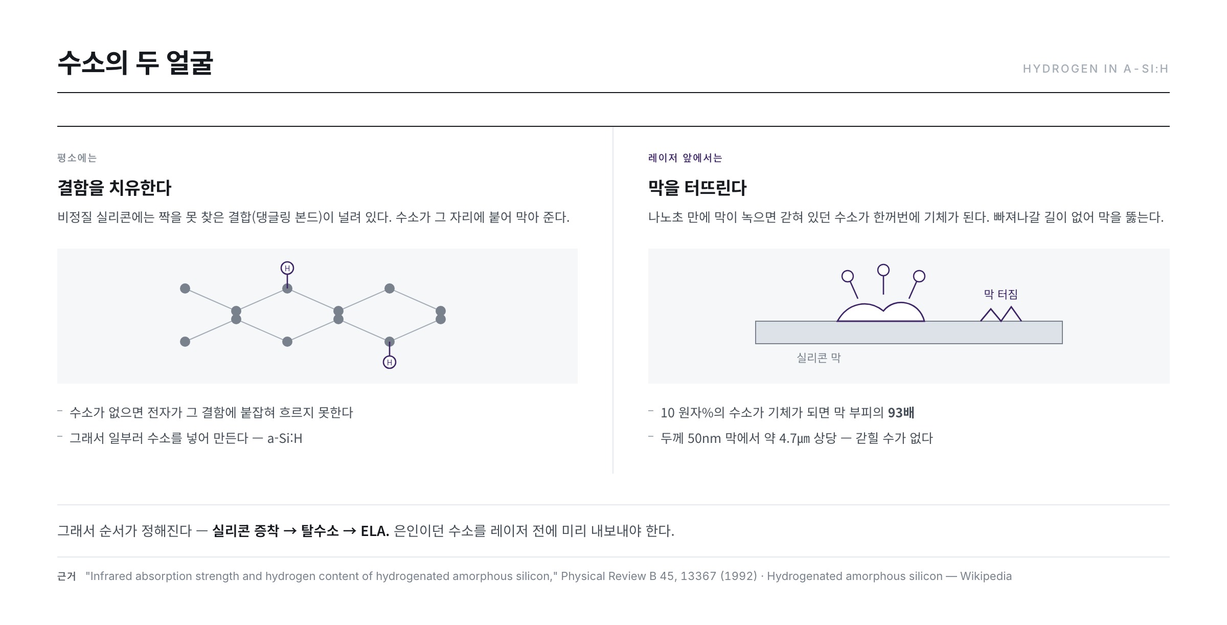
- The silicon-hydrogen bond is comparatively weak, so hydrogen is released first as temperature rises.
- The ELA laser melts the film in tens of nanoseconds — there is no time for hydrogen to escape.
- Trapped hydrogen vaporises instantly and pushes the film apart from inside.
The phenomenon appears in the literature in exactly these terms — "to prevent ablation caused by sudden hydrogen eruption during crystallisation of hydrogenated amorphous silicon thin films, a dehydrogenation anneal that lowers the hydrogen content is performed before crystallisation" (SID Symposium Digest, "LTPS Device and Panel Fabrication Using Excimer Laser Dehydrogenation and Crystallization", 2021). The same paper records that conventional dehydrogenation requires temperatures above 430~470℃, and reports that after dehydrogenation the hydrogen in the a-Si falls to about 0.6 at.%, improving both crystallisation and electrical characteristics.
How dangerous this is can be checked by arithmetic. Taking the atomic density of amorphous silicon as about 5×10²² atoms/㎤ and assuming all the hydrogen in the film emerges as H2 molecules, converting that gas to standard conditions gives the following.
| Hydrogen content | H2 molecule density | Volume at standard conditions | For a 50nm film | Expected in ELA |
|---|---|---|---|---|
| 2 at.% | 5.0×10²⁰ /㎤ | about 19× the film volume | equivalent to about 0.9㎛ | surface roughening, micropores |
| 5 at.% | 1.2×10²¹ /㎤ | about 47× the film volume | equivalent to about 2.3㎛ | eruption marks, local delamination |
| 10 at.% | 2.5×10²¹ /㎤ | about 93× the film volume | equivalent to about 4.7㎛ | ablation (the film bursts) |
| 15 at.% | 3.8×10²¹ /㎤ | about 140× the film volume | equivalent to about 7.0㎛ | widespread damage |
If all the hydrogen trapped in a 50nm film turns to gas, at room temperature and pressure it amounts to more than 90 times the film thickness in volume. In reality it expands momentarily inside molten silicon so the figure does not appear literally, but the difference in scale is unmistakable — with that much gas produced on a nanosecond timescale, the film has no way to hold together.
There is no time — a collision of two timescales
The real reason hydrogen becomes dangerous is not the content but the time. The same hydrogen leaves quietly if heated slowly. A dehydrogenation bake runs on a scale of tens of minutes — 30 minutes is 1,800 seconds. The time the film spends molten during ELA, by contrast, is around 100 nanoseconds, that is 0.0000001 second.
time ratio = 1,800 s ÷ 0.0000001 s = about 18 billion
For hydrogen to leave the film it must diffuse to the surface, and diffusion distance scales as the square root of time. So if the time shrinks by 18 billion, the diffusion distance shrinks by its square root — about 1/130,000. Hydrogen that could traverse the whole film thickness during a dehydrogenation bake is effectively frozen in place under ELA conditions.
The conclusion is clear. ELA cannot be the step that removes hydrogen. Hence the fixed order — silicon deposition → dehydrogenation → ELA. The analogy is an egg in a microwave: boil it slowly and nothing happens, heat it abruptly and the steam inside cannot escape, so it bursts.
Incidentally, measuring effusion curves while varying the heating rate or film thickness allows the hydrogen diffusion coefficient in the film to be inferred ("Determination of the hydrogen diffusion coefficient in hydrogenated amorphous silicon from hydrogen effusion experiments," Journal of Applied Physics 53, 8745 (1982)). The temperature and time of a dehydrogenation recipe are ultimately designed on top of that diffusion coefficient.
The three faces of thermal processing
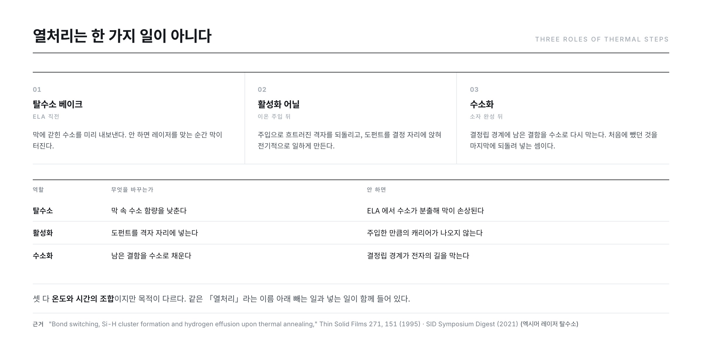
In backplane processing the act of "baking" appears several times for different purposes. Drawing the map in advance makes the later articles much easier.
| Step | When | Hydrogen is | Purpose | If overdone |
|---|---|---|---|---|
| ① Dehydrogenation bake | Right after silicon deposition, before ELA | removed | Keep the film from bursting under the laser | Substrate deformation, excess thermal budget |
| ② Activation anneal | Right after doping (Part 8) | not involved | Lattice recovery + dopant activation | Dopant diffuses where it should not |
| ③ Hydrogenation | Late, once the device is nearly done | added | Cap traps at grain boundaries | Excess hydrogen degrades characteristics |
② The activation anneal restores the silicon lattice disturbed by implanted ions and lets the implanted dopant atoms settle onto lattice sites and become electrically active. Recovery and activation must be achieved in a single heating, and overdoing it spreads the dopant, so the balance of temperature and time is the crux (Ion implantation). ③ Hydrogenation is the opposite: hydrogen is deliberately put back in, capping the broken bonds remaining at the grain boundaries of polycrystalline silicon so the transistor finishes with a threshold voltage that does not drift.
Though all are "heating", ① is opening an escape route for gas, ② is re-laying disturbed bricks, and ③ is applying finishing putty. Hydrogen is an element with times to remove and times to add, managed throughout the process.
Hydrogen even obstructs crystal growth
Dehydrogenation is not only about preventing explosions. The second reason is that remaining hydrogen suppresses grain growth.
During ELA, grains rearrange under repeated irradiation such that small ones vanish and large ones grow (secondary grain growth, detailed in Part 6). But if hydrogen attaches at a grain boundary it forms a hydrogen-vacancy pair and blocks the path along which atoms would move. The result is that films with more residual hydrogen end up with smaller grains. Keeping residual hydrogen down to the 1~2 at.% level in real processes is therefore not only about preventing bursts but also about obtaining large grains.
Interestingly, the hydrogen content of the buffer layer (nitride family) beneath the a-Si has the same kind of influence, because hydrogen rising from the layer below can obstruct crystal growth — meaning the hydrogen budget of the whole stack, not of one film, must be managed. The relationship between annealing conditions and the state of hydrogen in the film has been a subject since the early literature ("Thermal annealing and hydrogenation of chlorinated hydrogenated amorphous silicon," Thin Solid Films 147, 285 (1987)).
How it is removed — the available options
The goal of dehydrogenation is simple — reduce hydrogen enough for ELA to survive, within the temperature the substrate can bear. There are broadly three options.
| Approach | Condition | Residual hydrogen reached | Advantage | Risk |
|---|---|---|---|---|
| Straight to ELA, no dehydrogenation | — | a few % to over 10% | Shorter process | Ablation from hydrogen eruption |
| Furnace dehydrogenation (conventional) | above 430~470℃, tens of minutes | about 0.6 at.% | Good large-area uniformity | Long process time, substrate thermal budget |
| Low-energy laser pre-irradiation | fluence below crystallisation | improved crystallisation reported | Both steps in the same chamber | Too little energy leaves hydrogen; too much ablates |
The figures in the table are those given in the SID 2021 report cited above. The third row is the recent attempt: irradiate first with an excimer laser at low energy to drive hydrogen out, then immediately at high energy to crystallise, so that both steps run consecutively in the same chamber. The power-density window is narrow, however — too little and dehydrogenation is incomplete, too much and the film ablates. Irradiation at high energy density is indeed reported to make amorphous silicon films agglomerate into islands, which shows the upper bound is real ("Agglomeration of amorphous silicon film with high energy density excimer laser irradiation," Thin Solid Films 515, 2872 (2007)).
There are also designs patented to prevent the substrate from being exposed to air at all between dehydrogenation and crystallisation — a patent titled "Method for crystallizing semiconductor material without exposing it to air" is one example (US 6,881,615 B2). A freshly dehydrogenated silicon surface is highly reactive, so ambient control in that interval affects crystallisation quality.
How do we know how much is left
Whether dehydrogenation worked is judged by measuring the residual hydrogen. But hydrogen is the lightest element and is poorly detected by ordinary analysis, so methods are chosen according to purpose.
| Method | What it looks at | Strength | Limitation |
|---|---|---|---|
| Infrared spectroscopy (FTIR) | Absorption strength at 2000 and 2090 cm⁻¹ | Distinguishes bonding form (SiH vs SiH2) | Needs a calibrated constant; blind to unbonded H2 |
| Raman spectroscopy | Disappearance of the Si-H peak, crystallinity | Non-destructive, easy on the line | Weak quantification |
| Hydrogen effusion measurement | Total H2 released during the ramp | Total amount and release temperature at once | Consumes the sample, not real-time |
| SIMS | Hydrogen distribution in depth | Profiles down to interfaces and the buffer | Destructive, needs a standard |
| ERDA (elastic recoil detection) | Energy of recoiled hydrogen atoms | Close to absolute quantification without standards | Needs an accelerator, hard on the line |
The most common combination on the floor is FTIR for bonding state and Raman for process judgement. Converting infrared absorption strength into hydrogen content requires a proportionality constant, and the study that measured and tabulated those values remains the standard reference today (Physical Review B 45, 13367 (1992) · "Si–H bonding in low hydrogen content amorphous silicon films," Journal of Applied Physics 87, 1650 (2000)). When an absolute figure is needed, ERDA provides a cross-check ("Quantitative analysis of hydrogen in thin films using Time-of-Flight ERDA," Thin Solid Films 518, 2617 (2010)). It is in this context that the report cited earlier states dehydrogenation is judged by the disappearance of the silicon-hydrogen peak near 2000 cm⁻¹.
The temperature ceiling — why it is a "low temperature" process
In semiconductor wafer processing an anneal around 1000℃ is unremarkable. Displays cannot do that. Glass substrates begin to deform and shrink from roughly 600℃, and a flexible PI substrate has an even lower limit. Recalling from Part 2 that substrate PI is specified at a glass transition of 390℃ or higher and finishes curing in the 400℃ range, one sees how tight a window 430~470℃ dehydrogenation really is.
So every anneal in the backplane is designed beneath this ceiling — the "LT (Low Temperature)" of LTPS is precisely the product of that constraint (Low-temperature polycrystalline silicon). The ELA of the next chapter chose a laser approach that "melts only the film surface momentarily without heating the substrate" for the same reason. The 1986 report that crystallised amorphous silicon with an excimer laser to make thin-film transistors was the start of that detour ("XeCl Excimer laser annealing used in the fabrication of poly-Si TFT's," IEEE Electron Device Letters 7, 276 (1986)).
What the floor watches — three control points
- Residual hydrogen concentration — the success or failure of dehydrogenation itself. Too little and the film is damaged in ELA; excessive temperature or duration deforms the substrate. The spectroscopic methods in the table above are the standard verification.
- Temperature uniformity — if temperature differs from place to place across the substrate, so does the amount of hydrogen left, and that difference becomes mottle in ELA crystallisation quality. The larger the area, the harder the fight.
- Ramp and cooling rate — too fast and the substrate bows and stress remains in the film. A fast ramp in particular densifies the surface first and traps the hydrogen underneath, so the temperature band where the effusion peaks stand must be crossed deliberately slowly. The principle of "slowly" seen in PI curing (Part 3) repeats here.
The next article (Part 5) compares the equipment that actually performs this heating — the furnace that bakes dozens of substrates at once, the continuous-transport in-line furnace, and RTA that reaches its peak in seconds — looking into the triangle of equipment choice: how many, how fast, up to what temperature.
References
- SID Symposium Digest of Technical Papers (2021) — "LTPS Device and Panel Fabrication Using Excimer Laser Dehydrogenation and Crystallization" : dehydrogenation to prevent ablation by hydrogen eruption, conventional 430~470℃, about 0.6 at.% hydrogen after dehydrogenation, disappearance of the 2000 cm⁻¹ peak
- "Infrared absorption strength and hydrogen content of hydrogenated amorphous silicon," Physical Review B 45, 13367 (1992) : standard reference for the constant converting absorption strength into hydrogen content
- "Si–H bonding in low hydrogen content amorphous silicon films as probed by infrared spectroscopy," Journal of Applied Physics 87, 1650 (2000) : Si-H bonding state in low-hydrogen films
- "Silicon-Hydrogen Bonding Configurations in Very Thin Hydrogenated Amorphous Silicon," Japanese Journal of Applied Physics 33, L1577 (1994) : distinguishing SiH, SiH2 and SiH3 configurations
- "Bond switching, Si-H cluster formation and hydrogen effusion upon thermal annealing," Thin Solid Films 271, 151 (1995) : multi-stage bond rearrangement and effusion during the ramp
- "Occurrence of Sharp Hydrogen Effusion Peaks of Hydrogenated Amorphous Silicon Film," physica status solidi (b) 257 (2020) : peak structure of the effusion curve
- "Determination of the hydrogen diffusion coefficient in hydrogenated amorphous silicon from hydrogen effusion experiments," Journal of Applied Physics 53, 8745 (1982) : inferring the diffusion coefficient from effusion experiments
- "Thermal annealing and hydrogenation of chlorinated hydrogenated amorphous silicon," Thin Solid Films 147, 285 (1987) : annealing conditions and the state of hydrogen in the film
- "Quantitative analysis of hydrogen in thin films using Time-of-Flight Elastic Recoil Detection Analysis," Thin Solid Films 518, 2617 (2010) : quantifying hydrogen without standards
- "Agglomeration of amorphous silicon film with high energy density excimer laser irradiation," Thin Solid Films 515, 2872 (2007) : film damage past the energy-density limit
- "XeCl Excimer laser annealing used in the fabrication of poly-Si TFT's," IEEE Electron Device Letters 7, 276 (1986) : early report of excimer laser crystallisation
- "Amorphous-silicon field-effect device and possible application," Electronics Letters 15, 179 (1979) : the origin of amorphous silicon field-effect devices
- US 6,881,615 B2 — Method for crystallizing semiconductor material without exposing it to air : blocking the ambient between dehydrogenation and crystallisation
- Hydrogenated amorphous silicon · Dangling bond · Ion implantation · Annealing · Low-temperature polycrystalline silicon — Wikipedia : hydrogen content of a-Si:H, dangling bonds, implantation damage and activation anneal, the LTPS process flow