We have finally reached the most dramatic process in this series. Its name is ELA (Excimer Laser Annealing). An ultraviolet laser melts and refreezes a silicon film within tens of nanoseconds — a moment about a million times shorter than a blink, in which the fate of the material is decided. It is the instant the "P" (polycrystalline) of LTPS is made, and the name LTPS exists because of this process.
Why go this far — the performance gap
The difference between amorphous and polycrystalline is not a matter of taste but a matter of orders of magnitude.
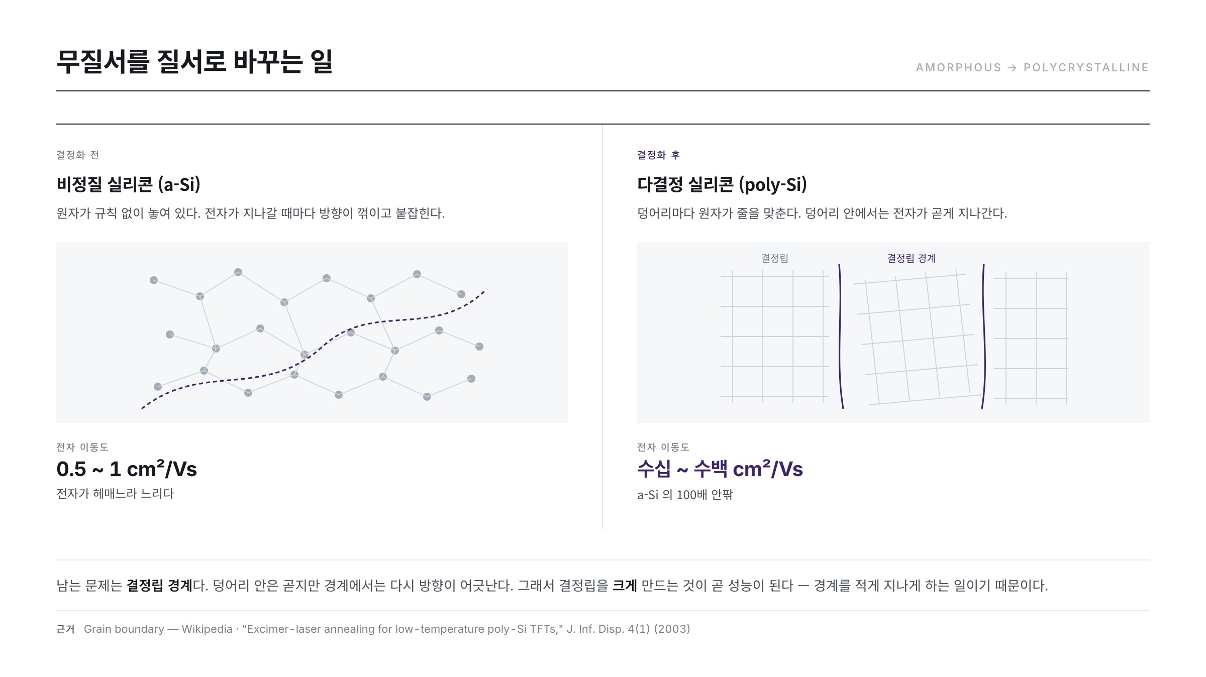
- Electron mobility — a-Si:H sits at 0.5–1 cm²/Vs, while LTPS climbs to a region roughly a hundred times higher.
- Hole mobility — a-Si makes P-type devices effectively impractical; LTPS makes them possible (CMOS becomes available).
- On/off current ratio — where a-Si is around 10⁵, LTPS exceeds 10⁹.
- What is lost in exchange — the uniformity a-Si was proud of. LTPS has wider spread in threshold voltage and mobility.
| Aspect | a-Si:H | ELA polycrystalline silicon | Nature of the difference |
|---|---|---|---|
| Atomic arrangement | Disordered (no long-range order) | A mosaic of grains | Structurally different |
| Electron mobility | 0.5–1 cm²/Vs | Tens to hundreds cm²/Vs | About 100× |
| P-type devices | Effectively impractical | Possible (CMOS) | Circuit design freedom |
| On/off ratio | About 10⁵ | Over 10⁹ | Four orders |
| Device-to-device spread | Small | Large (depends on grain boundary position) | LTPS is worse |
| Process steps | Few | Many (laser step added) | Cost difference |
From an electron's point of view, amorphous is a fog-bound gravel track and polycrystalline is a paved road. But the paved road has joints (grain boundaries), and those joints fall in different places from spot to spot — that is the fate of LTPS. The reason part 1 said "LTPS is overwhelming in mobility but loses on uniformity" is the fifth row of this table. It is no exaggeration to say that half of LTPS processing is a fight to win that uniformity back.
Why it has to be a laser
The simplest way to crystallise silicon is to bake it for a long time (solid phase crystallisation). But that is impossible for displays, because of the temperature ceiling seen in the previous article. Glass loses its shape above the strain point, and a flexible PI substrate is damaged at even lower temperatures.
A laser resolves this dilemma elegantly. The key is "only the surface, only for an instant." An ultraviolet laser pulse is absorbed almost entirely within tens of nanometres of the silicon surface, melting only that thin layer momentarily. The absorption depth of silicon at 308 nm is under 10 nm, so even in a 50 nm silicon film the light ends near the surface.
But shallow absorption alone is not enough, because heat does not stay where it was absorbed. What proves decisive here is time. Heat spreads roughly √(D·t) in time t (D being thermal diffusivity), and at nanosecond scales that quantity becomes extremely small.
| Pulse width | Heat diffusion length in silicon | In glass | Meaning |
|---|---|---|---|
| 10 ns | about 0.92 μm | about 0.09 μm | Tens of times the silicon film thickness |
| 30 ns | about 1.60 μm | about 0.16 μm | Representative ELA condition |
| 50 ns | about 2.06 μm | about 0.21 μm | Long-pulse type |
| 200 ns | about 4.12 μm | about 0.42 μm | Heat begins leaking into the substrate |
The third column is this process's reason for existing. Glass has a thermal diffusivity around one hundredth that of silicon, so with a 30 ns pulse the heat penetrates less than 0.2 μm into the glass. With the glass around 0.5 mm thick, only about one 2,500th of it — the very top — is warmed at all. The result is that the silicon melts and refreezes above 1,400 °C while the glass beneath is barely heated. To the question posed in part 5 — "raise the temperature or extend the time?" — ELA answers by pushing the temperature to an extreme and the time to the opposite extreme.
A nanosecond timetable — from melting to freezing
Laying out what happens inside a single pulse, in order, makes the character of this process clearer.
- 0 to a few ns — absorption. Ultraviolet light excites electrons within 10 nm of the surface, that energy passes to the lattice, and the temperature soars.
- A few to tens of ns — melting. Melting begins at the surface and the melt front travels downward. How far it goes decides the energy density regime discussed next.
- Tens to hundreds of ns — solidification. Once the pulse ends, heat escapes downward and the film freezes from the bottom upward. The solidification front moves at metres per second — more than six orders faster than solidification in metal casting.
An important concept here is undercooling. Freezing this quickly, the liquid drops far below its melting point before solidification begins. The deeper the undercooling, the more nuclei appear simultaneously in many places, splitting the material into fine grains. Shallow undercooling instead lets existing seeds grow slowly into large grains. The four regimes that follow come down to a combination of how many seeds survived and how deeply the liquid was undercooled.
Energy density sets the grain size
So is a stronger laser always better? No. This is the most interesting part of ELA — the crystallisation behaviour changes completely with energy density.
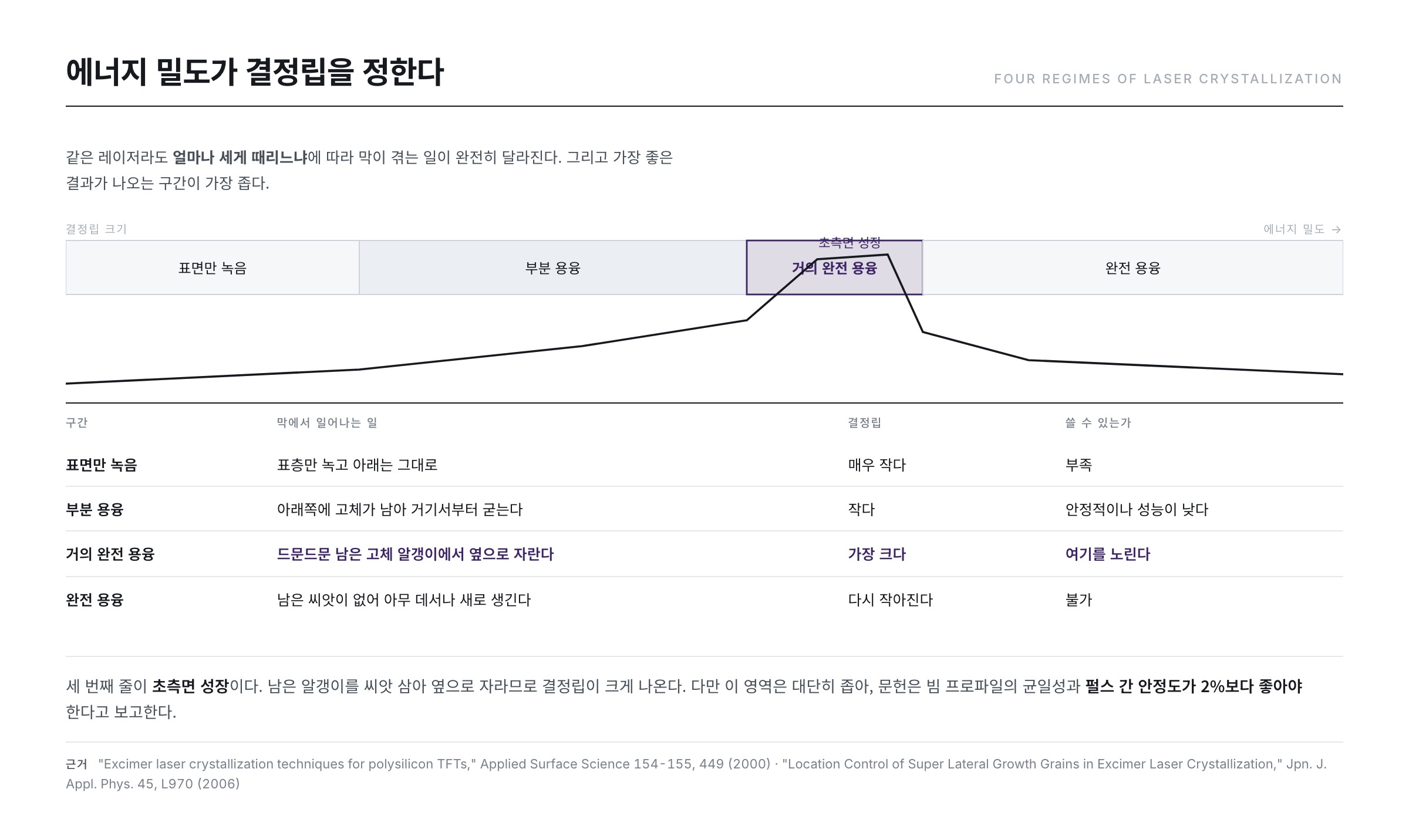
| Regime | Melt state | Crystallisation mechanism | Grain size | Assessment |
|---|---|---|---|---|
| 1. Low energy | Surface layer only | Explosive crystallisation | Very fine | Low mobility |
| 2. Partial melt | Upper part melts, lower part survives | Vertical growth from surviving seeds | Columnar, about the film thickness | Stable but unremarkable |
| 3. Near-complete melt | Only a few seeds survive | Super lateral growth | Larger than the film thickness, can exceed 1 μm | Optimal — but the window is narrow |
| 4. Complete melt | No seeds survive | Homogeneous nucleation after undercooling | Fine again | Mobility collapses |
This four-regime division is set out in the literature as well. Excimer laser crystallisation divides into the partial-melting region, the high-energy region above the complete-melting threshold, and the transition region between them, with the largest grains obtained through super lateral growth in that transition region — islands of unmelted silicon serve as seeds and regrow sideways from the liquid, letting grains exceed 1 μm.
The problem is that this region is brutally narrow. The literature reports the process window for super lateral growth at ΔE/E ≈ 0.025 — about 2.5 % of the energy. Part 5 said the controlled variable for RTA is "peak temperature accuracy rather than time"; ELA is far harsher. A few per cent of pulse-to-pulse energy jitter becomes mottling in grain size, and finally appears as brightness mura on the screen. Hence the saying that pulse-to-pulse energy stability is picture quality.
Not once but many times — overlapping shots
ELA moves a line-shaped beam in small steps so that the same spot is struck by several pulses. A single shot leaves grain size and orientation uneven, but melting and refreezing the same spot again rearranges things so that small grains disappear and large grains grow larger — secondary grain growth. Grains with favourable orientation absorb their neighbours as they grow.
How many shots a spot receives is set by the overlap ratio — how tight the scan pitch is relative to the beam width. The relation is simple: the number of hits is 1/(1 − overlap).
| Overlap | Hits per spot | Scan pitch (400 μm beam) | Character |
|---|---|---|---|
| 50 % | 2 shots | 200 μm | Fast but insufficiently uniform |
| 80 % | 5 shots | 80 μm | — |
| 90 % | 10 shots | 40 μm | — |
| 95 % | 20 shots | 20 μm | Typical operating region |
| 98 % | 50 shots | 8 μm | Good uniformity, throughput collapses |
What the table shows is an honest exchange between quality and throughput. Raising overlap from 95 % to 98 % — three percentage points — takes the shots per spot from 20 to 50, a factor of 2.5, and stretches the time to process one substrate by the same factor. This table is why the ELA tool is called the bottleneck of the line.
Here the previous article comes back. Hydrogen left in the film obstructs this secondary growth — experiments report that hydrogen impedes atomic motion at grain boundaries and slows growth. That is why the dehydrogenation of part 4 is not only about preventing blistering but about the crystal quality itself. A thin native oxide on the surface is reported to block growth the same way, which makes surface condition immediately before ELA a matter of consequence.
Paths to crystallisation — ELA is not the only one
ELA is not the only way to turn amorphous into polycrystalline silicon. Seeing what each method gives and gives up makes it clear why ELA became the mass-production standard.
| Method | Principle | Temperature and time | Grains | Limitation |
|---|---|---|---|---|
| Solid phase crystallisation (SPC) | Rearrangement in the solid state through long heating, without melting | 600 °C class · hours to tens of hours | Fine, many defects | Runs into the glass strain point; the time is impractical |
| Metal-induced crystallisation (MIC/MILC) | A metal catalyst lowers the crystallisation temperature | Around 500 °C · hours | Long and narrow crystals | Residual metal contamination; higher device leakage |
| ELA | Nanosecond pulses melt and refreeze only the surface layer | Momentarily above 1,400 °C · tens of ns | 0.3–1 μm class | Narrow energy window; mura is hard to manage |
| Sequential lateral solidification (SLS) | Narrow slits divide the beam to force the growth direction | Same band as ELA | Several μm, oriented | Many scans, so low throughput |
The first two rows explain why the field went to lasers: glass cannot survive solid phase crystallisation, and metal-induced crystallisation leaves catalyst behind. The last row explains why ELA is used even though better methods exist — techniques that grow larger grains and even align their direction do exist, but they multiply the number of scans beyond what large-area mass production can absorb. ELA is not the method that gives the best crystal quality; it sits at the ceiling of quality that mass production can afford.
Grain boundaries — the fate of polycrystals
Polycrystalline silicon is a mosaic of grains stuck together, so grain boundaries form between them. A boundary is where atomic arrangement breaks down, so vacancies and dangling bonds cluster there; when charge is trapped, a potential barrier appears for electrons to climb. Speed bumps along the paved road.
Simple arithmetic shows why grain size matters so much. The number of boundaries an electron meets crossing a transistor channel is channel length ÷ grain size.
| Grain size | 3 μm channel | 5 μm channel | 10 μm channel |
|---|---|---|---|
| 0.05 μm | 60 | 100 | 200 |
| 0.1 μm | 30 | 50 | 100 |
| 0.3 μm | 10 | 17 | 33 |
| 1 μm | 3 | 5 | 10 |
| 3 μm | 1 | 2 | 3 |
Reading down the table shows why mobility jumps by orders. With 100 boundaries versus 3, the total barrier an electron faces is not comparable. But the more alarming cell is the bottom right. Only three boundaries also means device characteristics shift substantially depending on where those three happen to fall. With 100 boundaries the average smooths everything out and device-to-device differences stay small; with three it is like rolling a die three times, and the spread widens. Hence the paradox: growing grains improves average performance and degrades uniformity.
What about the boundaries that remain? Later, hydrogenation fills their dangling bonds with hydrogen — completing the irony of putting back, at the end, the hydrogen so painstakingly driven out at the start. The manner differs, though: what was removed was hydrogen spread through the whole film, while what is added targets the specific sites that are boundaries.
Common misconceptions
- "Stronger laser, bigger grains" — regime 4 is the counterexample. Once every seed is gone, undercooled liquid freezes everywhere at once and grains become finer. Overshooting the optimum degrades performance.
- "The glass doesn't melt, so there's no thermal problem" — the glass does not melt, but its top layer is heated, and that heating repeats dozens of times, once per pulse. Substrate distortion and stress from repeated thermal shock remain exactly as described in part 5.
- "Bigger grains are always better" — better for average mobility, worse for device-to-device spread. That is why OLED backplanes look at uniformity before grain size.
- "ELA is a single pass" — at 95 % overlap the same spot melts and refreezes twenty times. A given point experiences not one crystallisation but twenty recrystallisations.
What the floor watches
Turning the numbers above into control items gives the following.
- Pulse energy stability — with a process window of only 2.5 %, shot-to-shot energy variation is monitored continuously. As the laser medium ages the output drifts down, and the moment that drift leaves the window the grain structure changes wholesale. The trick is to watch the slope rather than the meter reading.
- Indirect measurement of grain state — you cannot section the film every time, so non-destructive methods are used. Surface reflectance and scattered light correlate with grain size, allowing an optical measurement to judge the result immediately on the line.
- Mura inspection — the final verdict is the visible mottling. Stripes along the scan direction point to overlap and pitch; irregular blotches point to pulse energy. The shape of the pattern names its cause.
- Optical contamination — molten silicon that splashes onto a lens or window lowers transmission, so the energy actually delivered quietly falls. The setpoint is unchanged while only the result degrades — a classic trap, which makes the cleaning interval for optical parts a matter of process stability.
Summary — and the next article
- ELA crystallises by melting only the surface for nanoseconds, without heating the glass. Glass having one hundredth the thermal diffusivity of silicon is what makes this possible.
- Grain size is a function of energy density, and the window at the optimum (super lateral growth) is only about 2.5 % wide.
- Overlapping shots grow the grains (20 shots at 95 % overlap), but residual hydrogen obstructs that growth.
- Growing the grains raises average performance and worsens uniformity. The remaining boundaries are pacified later by hydrogenation.
The next article (part 7) moves to the equipment that actually produces this laser — why 308 nm specifically, how a ragged beam is shaped into a uniform line beam, why scan pitch and overlap produce mura and moiré, and why oxygen is mixed into the gas flowing through the chamber.
References
- "Excimer laser crystallization techniques for polysilicon TFTs," Applied Surface Science 154-155, 449 (2000) : partial/complete melting and the transition region, super lateral growth and grains above 1 μm — source of the ΔE/E ≈ 0.025 process window quoted above
- "Surface melt dynamics and super lateral growth regime in long pulse duration excimer laser crystallization of a-Si films," Thin Solid Films 337, 143 (1999) : surface melt behaviour with pulse duration and the super lateral growth regime
- "Phase-field modelling of excimer laser lateral crystallization of silicon thin films," Thin Solid Films 427, 309 (2003) : numerical modelling of melt and solidification fronts and lateral growth
- "Location Control of Super Lateral Growth Grains in Excimer Laser Crystallization," Jpn. J. Appl. Phys. 45, L970 (2006) : approaches to controlling where super lateral growth grains form
- "New theory of undercooling during rapid solidification: application to pulsed laser," Applied Physics A 88, 179 (2007) : basis for the undercooling and solidification velocity in the nanosecond timetable above
- "Effect of Hydrogen on Secondary Grain Growth of Polycrystalline Silicon Films," Jpn. J. Appl. Phys. 45, 6908 (2006) : experimental evidence that residual hydrogen obstructs secondary grain growth — the link back to dehydrogenation in part 4
- "The grain growth blocking effect of polycrystalline silicon film by thin native oxide," Appl. Phys. Lett. 75, 460 (1999) : a thin native surface oxide blocking grain growth
- T. Sameshima, S. Usui, M. Sekiya, "XeCl excimer laser annealing used in the fabrication of poly-Si TFT's," IEEE Electron Device Letters 7(5), 276 (1986) : the first report of poly-Si TFTs made by excimer laser crystallisation
- "Excimer-laser annealing for low-temperature poly-Si TFTs," J. Inf. Disp. 4(1) (2003) : ELA process overview and TFT characteristics against a-Si — basis for the mobility comparison table above
- Excimer laser — Wikipedia : principles and wavelengths of excimer lasers
- Grain boundary — Wikipedia : structure of grain boundaries and their electrical effects
- Thermal diffusivity — Wikipedia : basis for the √(D·t) heat diffusion length used above