The previous article covered what ELA does — melting only the surface for nanoseconds to grow crystals. This article is about the equipment that actually performs that work. Following the path the light takes from the laser source to the substrate, we look at "why this wavelength", "why the optics are so elaborate", and the identity of the thing the floor fears most: stripe mura.
What an excimer laser is
The "E" in ELA stands for excimer, short for "excited dimer" — a molecule that can exist only briefly, and only in an excited state. A noble gas (xenon, krypton) and a halogen (chlorine, fluorine) that would not normally bond join hands for an instant under strong electrical energy, then separate again, spitting out that energy as an ultraviolet photon.
This "collapses as soon as it exists" property is actually favourable for a laser. With almost no molecules in the ground state, population inversion arises naturally and amplification comes easily. The combination sets the wavelength, and display crystallisation occupies only one of those slots.
| Gas combination | Wavelength | Photon energy | Main use |
|---|---|---|---|
| ArF | 193 nm | 6.4 eV | Semiconductor lithography, fine machining |
| KrF | 248 nm | 5.0 eV | Lithography, laser lift-off |
| XeCl | 308 nm | 4.0 eV | Display crystallisation (ELA) |
| XeF | 351 nm | 3.5 eV | Materials processing, research |
Why 308 nm specifically
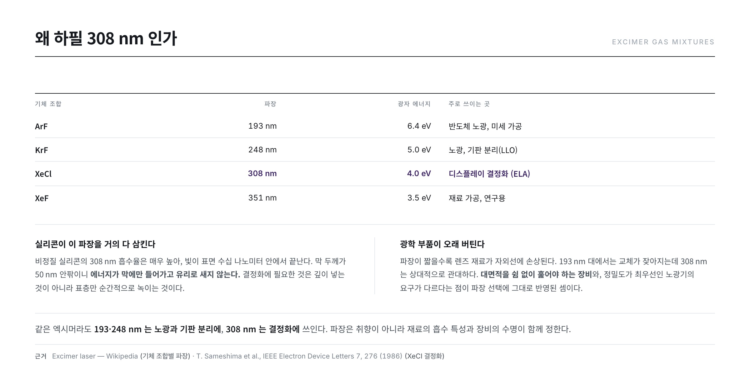
- Silicon swallows this wavelength almost entirely — amorphous silicon absorbs over 98 % at 308 nm, with an absorption depth of only tens of nanometres. The energy concentrates in a thin surface layer, making it possible to melt only the surface without heating the glass.
- Going longer, into the visible and infrared, silicon simply transmits the light and no surface heating occurs.
- High power can be produced stably — excimer lasers suffer from intermediate reaction products reabsorbing the light they emit, eating into output; the XeCl combination has relatively small losses of this kind.
- Among excimers, 193 nm and 248 nm serve semiconductor lithography and substrate lift-off; display crystallisation belongs to 308 nm.
There is one more practical reason. The shorter the wavelength, the shorter the life of the optical components. Around 193 nm, lens materials degrade under ultraviolet exposure and need frequent replacement, whereas 308 nm is comparatively forgiving — which favours running large-area equipment for long stretches. The differing demands of a lithography tool, where precision comes first, and a crystallisation tool, which must sweep large areas without pause, are reflected directly in the choice of wavelength.
The journey of the beam to the substrate
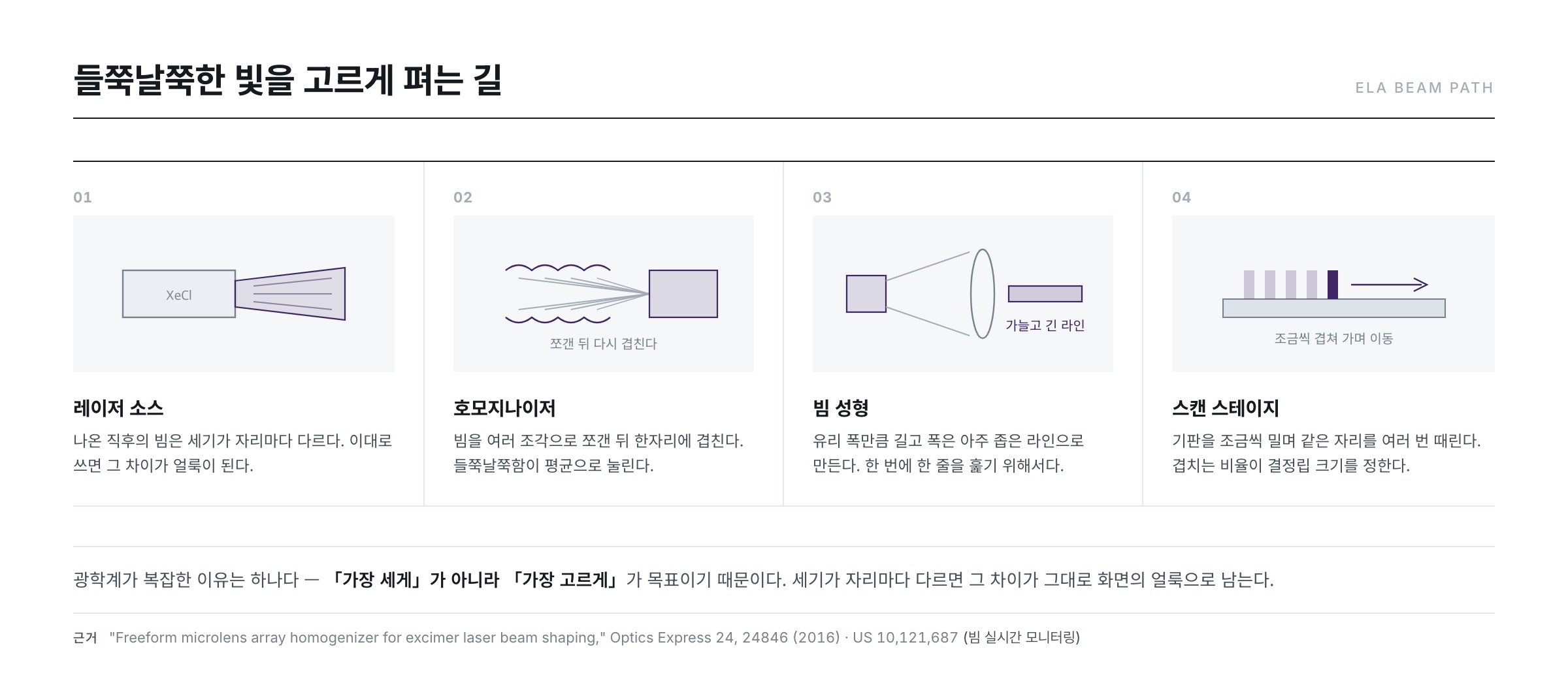
You cannot fire the light straight from the laser onto the substrate, because the intensity across its cross-section is uneven. As the previous article showed, the optimal energy window is only about 2.5 % wide, so a beam with a ragged profile becomes mottling directly. That is why most of the tool is optics.
- Homogeniser — splits the beam into many parts and overlays them again to flatten the intensity profile. Pressing a jagged ridgeline into a plateau. Research on freeform microlens arrays to push that flatness further continues today.
- Beam shaping optics — trims the flattened beam into a long, very thin line. The narrower it is, the easier to raise energy density; the longer it is, the wider the area swept per pass.
- Micro-smoothing mirror — excimer lasers have relatively low coherence, but interference fringes still form inside the optics. These are handled by vibrating a mirror slightly with a piezoelectric actuator to smear the fringes out in time.
- Scan stage — moves the substrate in precise small steps so the line beam sweeps the whole surface with overlap.
Why the beam must be a long thin line emerges from a simple division. Pulse energy divided by beam area is the energy density, and the optimal band from part 6 is roughly 300–450 mJ/cm².
| Line beam dimensions | Beam area | 0.5 J pulse | 1.0 J pulse | 1.5 J pulse |
|---|---|---|---|---|
| 465 × 0.4 mm | 1.9 cm² | 269 mJ/cm² | 538 mJ/cm² | 806 mJ/cm² |
| 750 × 0.4 mm | 3.0 cm² | 167 mJ/cm² | 333 mJ/cm² | 500 mJ/cm² |
| 1,500 × 0.4 mm | 6.0 cm² | 83 mJ/cm² | 167 mJ/cm² | 250 mJ/cm² |
Reading across shows that a longer beam demands a stronger source. Tripling the line from 465 mm to 1,500 mm requires tripling the pulse energy for the same energy density. Reading down shows why the width is squeezed to around 0.4 mm — doubling the width doubles the pulse energy required. What sets the size of a large-area tool is not the stage but the pulse energy of the source.
So the essence of an ELA tool is not "a powerful laser" but "optics that make it uniform plus a stage that moves it precisely." Indeed, the monitoring method itself is the subject of patents, which shows how central real-time surveillance of beam condition is to this equipment.
The arithmetic of throughput — why ELA is the bottleneck
Part 6 said the overlap ratio trades quality against throughput. Rendered in equipment numbers, that trade looks like this. Scan speed is scan pitch × repetition rate, so knowing the overlap and the shots per second gives it immediately.
| Overlap | Scan pitch | 300 Hz | 600 Hz | 1,200 Hz | Time to sweep 1,500 mm (600 Hz) |
|---|---|---|---|---|---|
| 90 % | 40 μm | 12.0 mm/s | 24.0 mm/s | 48.0 mm/s | about 63 s |
| 95 % | 20 μm | 6.0 mm/s | 12.0 mm/s | 24.0 mm/s | about 125 s |
| 98 % | 8 μm | 2.4 mm/s | 4.8 mm/s | 9.6 mm/s | about 312 s |
Three things stand out. First, the scan speed is millimetres per second — to the eye it crawls, almost stationary. Second, raising the overlap from 95 % to 98 % takes 2.5 times as long to sweep the same substrate. Third, the only lever that offsets this is repetition rate. That is why continuous kHz-class operation of discharge-pumped XeCl lasers has been researched for decades — doubling the repetition rate halves the processing time.
Lines therefore respond in another direction as well, placing several ELA tools side by side and alternating substrates between them, or splitting one substrate into zones processed in parallel. Adding tools introduces a new problem, however: tool-to-tool variation. With identical setpoints, differences in source gas condition and optics state shift the grain structure subtly, and that difference surfaces within a single substrate as mottling at the zone boundaries. Buying throughput by adding tools means paying for it in uniformity, which makes capacity expansion a question of quality design rather than a simple investment decision.
Raising the repetition rate has its own price, though. Firing more often into the same volume consumes gas and electrodes faster and makes pulse-to-pulse energy variation harder to control. The narrow 2.5 % window from part 6 becomes harder to hold the faster you run. The faster it runs, the more uniformity wavers — that is the fundamental tension of this tool.
Laser gas is a consumable
One fact about excimer lasers is often overlooked: the substance that emits the light wears out. Unlike the crystal of a solid-state laser or the chip of a semiconductor laser, the emitter of an excimer laser is the gas mixture filling the chamber.
In the XeCl combination it is mainly the halogen that is consumed. As discharges repeat, chlorine reacts with electrode metal and chamber walls and gradually disappears, while reaction by-products and impurities accumulate in its place. Two consequences follow — output drifts down, and pulse-to-pulse energy variation grows. Given the 2.5 % window from part 6, the second is the more dangerous. A slightly lower average can be compensated by raising the voltage; increased jitter cannot be compensated at all.
Operation therefore splits into two levels. Partial replenishment, topping up only the halogen to restore output, is done periodically; once impurities accumulate, the whole chamber undergoes a full gas change. Electrodes are replaced on a much longer cycle, but as they erode the discharge skews to one side and tilts the intensity profile across the beam — producing the stripes parallel to the scan direction seen later. Tracing a mura back to its cause frequently leads past the optics and lands, in the end, on the consumption state of the source.
Stage precision is pitch precision
However good the optics, they are useless if the stage carrying the substrate wavers. How precise it must be follows from multiplying the two numbers above.
At 95 % overlap the scan pitch is 20 μm and a given point receives 20 shots. But if the pitch is off by even 1 μm, the shots that point receives shift from 20 to 19 or 21 — a change of 5 %. With the optimal window at 2.5 %, a 1 μm positioning error alone already overshoots the window twofold.
Working backwards gives the requirement. To keep cumulative energy variation within 1 %, half the window, the pitch error must stay within 0.2 μm. That precision must hold across a 1,500 mm sweep, which relative to the full travel is one part in a million. This is why an ELA tool is called an assembly of precision stage technology, and why vibration, thermal drift and substrate warpage all become control items.
ELA mura and moiré — what the floor fears most
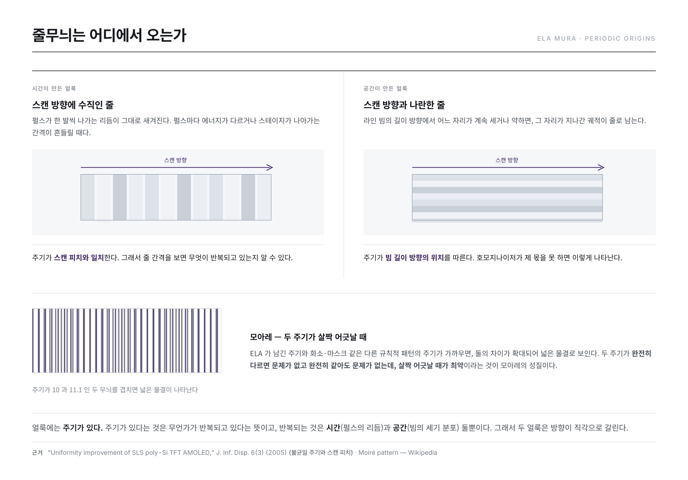
The signature defect of ELA is stripe mura. Regular brightness differences appear perpendicular to the scan direction, and the root cause is ultimately one thing — when crystal structure, grain size and boundaries differ from place to place, TFT performance differs, and that difference shows on screen as a brightness difference. The literature likewise reports that "the period of the brightness non-uniformity coincides exactly with the scan pitch."
That single sentence is the core of diagnosis. Mura has a period, and that period names the cause.
| Appearance | Period | Cause indicated | First response |
|---|---|---|---|
| Stripes perpendicular to scan | Matches scan pitch | Pulse-to-pulse energy variation, pitch error | Stabilise energy, re-tune pitch |
| Stripes parallel to scan | Position along beam length | Intensity profile across the line beam | Align and clean the homogeniser |
| Broad wave pattern | Difference against pixel pitch | Interference between ELA period and pixel period | Tilt the scan by 1–3° |
| Irregular blotches | None | Particles, local defects | Strengthen upstream cleaning and inspection |
The third row is moiré. When the period ELA leaves behind is close to another regular pattern such as the pixel or mask period, the difference between them is magnified into a broad wave. Two completely different periods cause no problem, and two identical periods cause no problem either; slightly mismatched is the worst case — that is the nature of moiré. Hence the response is not "match the periods" but "tilt the scan by 1–3° so the periods mismatch decisively."
Flowing gas — oxygen as seasoning
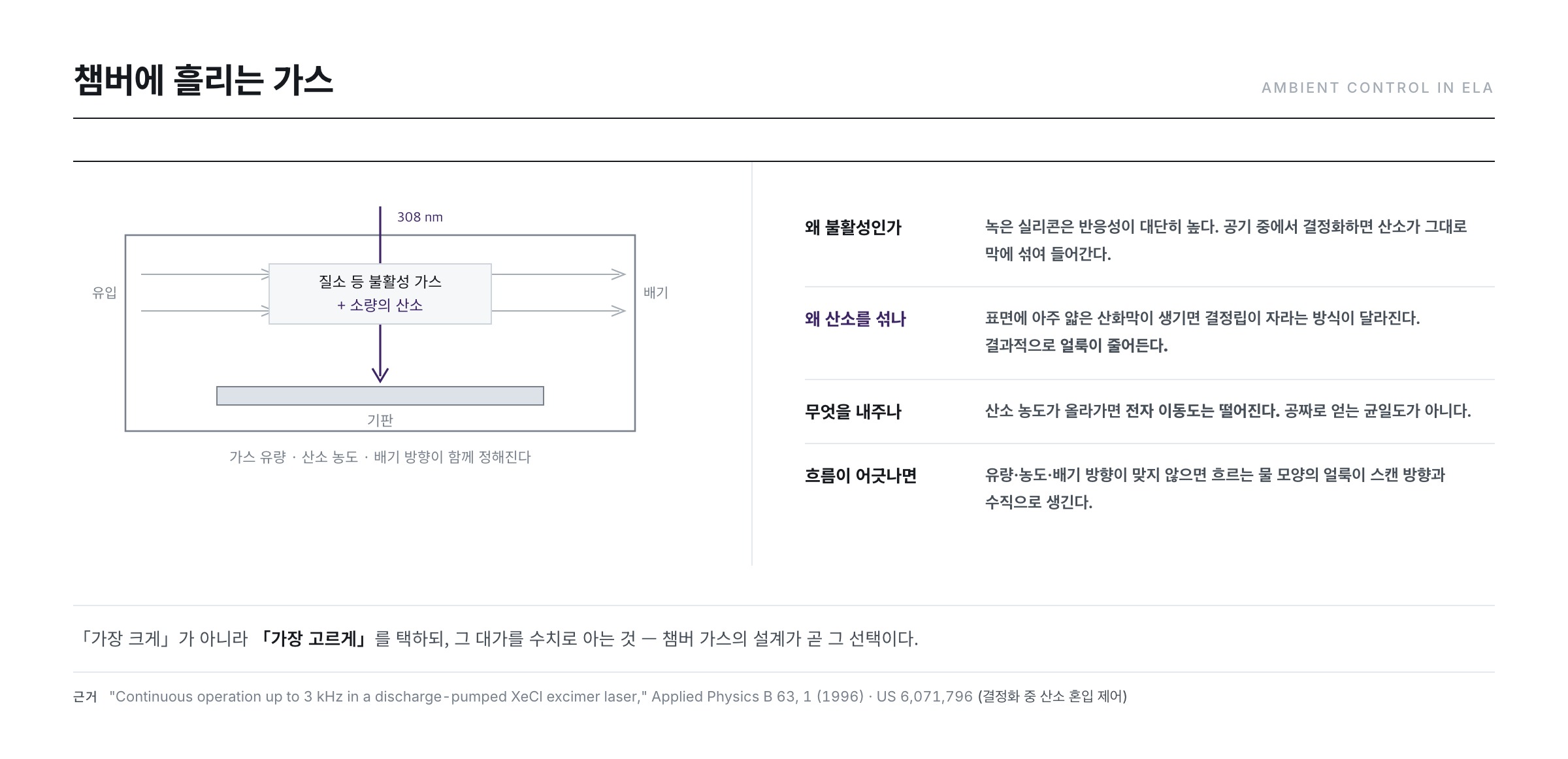
Gas flows through the ELA chamber, usually an inert gas such as nitrogen — into which a small amount of oxygen is deliberately mixed. The reason seems paradoxical at first: to suppress grains from growing too large.
Why suppress, when the previous article said larger grains are better? The answer is uniformity. As the table in part 6 showed, larger grains mean fewer boundaries in the channel, which widens device-to-device variation. A trace of oxygen restrains growth moderately and tidies the distribution. Controlling oxygen incorporation during crystallisation is, in fact, the subject of patents.
The cost is equally clear. As oxygen concentration rises, electron mobility falls. And if gas flow, oxygen concentration and exhaust direction are misaligned, flowing-water-shaped mottling appears perpendicular to the scan direction. Choosing "as uniform as possible" rather than "as large as possible", while managing the price numerically — that is what an ELA recipe really is.
An invisible bomb — particles underneath
Another failure mode is particles hidden beneath the silicon layer. Metal or foreign particles embedded in the PI surface or the buffer layer cause no trouble ordinarily, then create an accident at the instant of ELA.
The mechanism runs like this. As crystallisation proceeds the optical properties of silicon change and the laser penetrates deeper, delivering energy to the particle below. The locally overheated spot billows or bursts, deforming the surface, and that spot is later locally over-doped in the doping step, turning on at a lower voltage than its surroundings. The result is a bright dot on screen. The reason so much care goes into cleaning and inspection in the earlier steps (parts 2 and 3) surfaces here, several articles later.
The response is precise control of beam focus and intensity. The depth of focus of a XeCl source is around ±150 μm, so if the substrate bows outside that range or the stage wavers, the energy density immediately leaves the window. The thermal-stress-induced substrate warpage from part 5 becomes a problem again here — a management failure upstream eats into the tool's focus margin several steps later.
How do you look at the beam?
We said the energy density is monitored — but how do you measure an ultraviolet line 0.4 mm wide? There are layers to this too.
- Total energy — a fraction of the beam is split off along the path and caught by an energy meter. A value comes out for every pulse, so jitter is visible in real time, but it says nothing about how that energy is distributed along the line.
- Cross-sectional profile — a beam profiler captures the transverse intensity distribution. Whether the homogeniser is doing its job, and whether the profile has tilted to one side, shows up here. It requires stopping the tool, so this is periodic inspection rather than continuous surveillance.
- Working backwards from the result — the most reliable check is to sweep a test piece once and look at its surface. Crystallised regions change optically, so their reflectance shifts, and the shape and period of the mottling report the state of the beam directly.
The relation between the three layers is what matters. Total energy is fast but coarse, the profile is precise but slow, and observing the result is truthful but already too late. So the floor overlays all three — watching the trend in total energy continuously, checking the profile periodically, and narrowing the cause with a test piece when mura appears. The mura diagnosis table above works in practice only because that third layer exists.
What the floor watches — three control points
- Energy density monitoring — the lifeblood of ELA. Real-time output surveillance and periodic measured calibration keep the process inside the narrow optimum. Since gas life and electrode erosion drag the output down gradually, the trend matters more than the absolute value.
- Grain size and uniformity — samples are taken periodically for cross-sectional observation, with several panels and several points sampled across the substrate. The goal is not "large grains" but "uniform grains within a defined range."
- Source and optics condition — laser gas life, contamination and degradation of mirrors and lenses, stage travel accuracy. These three worsen quietly and then surface one day as mura, so managing the preventive maintenance cycle is quality management.
The substrate now carries a polycrystalline silicon film with large grains. But it is not yet a transistor — polarity must be written into it, marking which region is a channel and which is a switch. The next article (part 8) is doping.
References
- US 10,121,687 — Monitoring method and apparatus for control of excimer laser annealing : real-time beam monitoring for ELA control
- US 6,071,796 — Method of controlling oxygen incorporation during crystallization of silicon film by excimer laser : controlling oxygen incorporation during crystallisation
- US 6,881,615 B2 — Method for crystallizing semiconductor material without exposing it to air : ambient control during crystallisation
- "Freeform microlens array homogenizer for excimer laser beam shaping," Optics Express 24, 24846 (2016) : homogeniser optics that flatten the beam profile
- "Continuous operation up to 3 kHz in a discharge-pumped XeCl excimer laser," Applied Physics B 63, 1 (1996) : high repetition rate continuous operation of a XeCl source — basis for the repetition rates in the throughput table
- "Uniformity improvement of SLS poly-Si TFT AMOLED," J. Inf. Disp. 6(2), 20 (2005) : report that the period of brightness non-uniformity matches the scan pitch
- "Low-Temperature Poly-Si TFT by Excimer Laser Annealing," MRS Proceedings 685 (2001) : relation between ELA conditions and TFT characteristics
- "A new high-performance poly-Si TFT by simple excimer laser annealing," IEDM (2001), 34.3.1 : device characteristics improved through better crystallisation conditions
- "Excimer laser crystallization techniques for polysilicon TFTs," Applied Surface Science 154-155, 449 (2000) : ELA process window and uniformity — basis for the 300–450 mJ/cm² band used above
- Excimer laser — Wikipedia : wavelengths by gas combination — basis for the wavelength table above
- Excimer — Wikipedia : the concept of an excited dimer
- Moiré pattern — Wikipedia : patterns arising from interference between two periodic structures