So far we have built the substrate (Parts 2 and 3), prepared the silicon (Parts 4 and 5), and turned it into crystal (Parts 6 and 7). But crystallised silicon is still nothing more than a pure semiconductor. To become a transistor, it needs to be told where the electrons flow and where the switch sits — the polarity has to be written into the film. The process that does this is doping.
Impurities decide the character
Doping is exactly what the name says: deliberately planting impurities in silicon. Pure silicon barely conducts, but a trace of another element creates carriers that transport charge, and conductivity appears (Doping (semiconductor)).
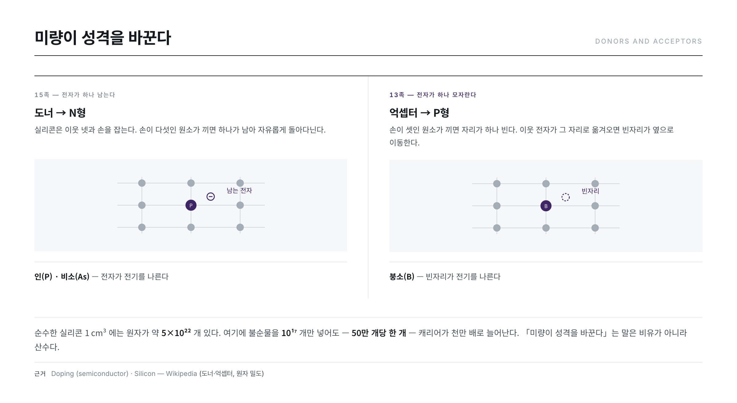
- Donor — a group 15 (V) element with one more outer electron than silicon (phosphorus, arsenic, antimony). It gives up the spare electron and produces N-type material.
- Acceptor — a group 13 (III) element with one electron fewer (boron, aluminium, gallium). It creates a missing electron, a hole, and produces P-type material.
An LTPS backplane makes both polarities, because the pixel driving circuit needs N-type and P-type devices side by side. The advantage noted back in Part 6 — that LTPS also secures hole mobility, so P-type devices become possible — is cashed in right here. Doping is therefore not a single step but several steps with different elements.
How much is "heavily doped"?
The most counter-intuitive thing about doping is the amount. What actually goes in is roughly one impurity atom per few hundred to a few hundred thousand silicon atoms. Let us check with numbers why that is enough. Silicon has a density of 2.329 g/cm³ and an atomic weight of 28.09 g/mol (Silicon), so the atomic density follows directly:
Silicon atomic density = 2.329 ÷ 28.09 × 6.022×10²³ ≈ 4.99×10²² cm⁻³
By contrast, the carriers that appear spontaneously in pure silicon at room temperature number only about 10¹⁰ cm⁻³ — roughly one carrier per five trillion atoms. Add impurities at just 10¹⁷ cm⁻³ and the carrier population jumps by seven orders of magnitude. "A trace changes the character" is not a metaphor; it is arithmetic.
What the process engineer actually sets is the dose, the number of ions driven in per unit area (cm⁻²).
average concentration = dose ÷ film thickness / sheet resistance Rs = 1 ÷ (q × mobility × concentration × film thickness)
The table below is a first-order estimate for a 50 nm polycrystalline silicon film, assuming every dopant is activated and fixing the mobility at 30 cm²/V·s. In reality mobility varies with concentration and the activation fraction is not 100%, so read the spacing between the orders of magnitude rather than the absolute values.
| Purpose | Dose (cm⁻²) | Average concentration (cm⁻³) | Relative to Si atoms | Sheet resistance (Ω/sq, approx.) |
|---|---|---|---|---|
| Channel doping (Vth adjustment) | about 1×10¹² | 2.0×10¹⁷ | 1 in 250,000 (4 ppm) | about 2×10⁵ |
| LDD doping (buffer region) | about 1×10¹³ | 2.0×10¹⁸ | 1 in 25,000 (40 ppm) | about 2×10⁴ |
| Source/drain doping | about 1×10¹⁵ | 2.0×10²⁰ | 1 in 250 (0.4%) | about 2×10² |
What the table really says is simple: raise the dose by three decades and the resistance falls by three decades. Source and drain must carry current, so their resistance has to be low; the channel must conduct only when the gate says so, so its resistance has to be high. Producing both extremes with the same tool and the same element, changing nothing but the dose, is the essence of the doping process.
Why these particular elements
Not just any group 13 or 15 element will do. The atom has to sit properly on a lattice site (solid solubility), stop at the intended depth (mass), and not smear too far during later heat steps (diffusivity).
| Element | Group / polarity | Atomic weight | Relative behaviour | Role in the backplane |
|---|---|---|---|---|
| Boron (B) | 13 / P-type | 10.81 | Lightest — travels deepest at a given energy, most prone to channelling | P-type devices, Vth adjustment |
| Phosphorus (P) | 15 / N-type | 30.97 | Mid mass — good balance of depth and damage | N-type source/drain, LDD |
| Arsenic (As) | 15 / N-type | 74.92 | Heavy — shallow, steep profile, heavy lattice damage | Where a shallow junction is required |
A backplane film is only about 50 nm thick. This is not a wafer stage where several micrometres are available, so there is almost no headroom in "depth". That makes keeping the acceleration energy low more important than the choice of element — if the dopant passes through the film and lands underneath, that is not doping, just penetration.
The three jobs of doping
In backplane manufacturing, doping steps are named after their purpose.
- Source/drain doping — forms the two terminals at either end of the transistor through which current enters and leaves. Doped heavily to lower the resistance.
- Channel doping — dopes the entire current path very lightly. The purpose is not conduction but moving the threshold voltage (Vth). Vth is set by the flat-band voltage, the surface potential and the depletion region; channel doping shifts the flat-band term, which moves the threshold without degrading the rest of the device characteristics.
- LDD (Lightly Doped Drain) doping — places a lightly doped buffer between the source/drain and the channel. By preventing the electric field from concentrating at a single point, it reduces leakage current and degradation.
LDD deserves a longer look. The chronic weakness of a polycrystalline silicon transistor is current that leaks when the device should be off: when the field crowds at the drain-side junction, electrons climb across using defect states at the grain boundaries as a ladder. Inserting a low-concentration region between source/drain and channel spreads the potential drop across that region and lowers the peak field. The literature reports measured leakage behaviour that differs with structure for polycrystalline silicon devices built with offset and LDD geometries ("Photo-Leakage Current of Poly-Si Thin Film Transistors with Offset and Lightly Doped Drain Structures," Jpn. J. Appl. Phys. 38, 5757 (1999)). The structure was explicitly claimed in early patents, and the question of the order in which the LDD region should be formed has remained patent subject matter ever since (US 5,698,882 — LDD Polysilicon thin-film transistor).
There is a price. Because the LDD region is resistive, it also reduces the on-current. Make it longer and leakage falls further but drive capability suffers; and since its length is set by lithographic alignment accuracy, LDD design ends up trading device performance against exposure margin.
Two ways in — diffusion and ion implantation
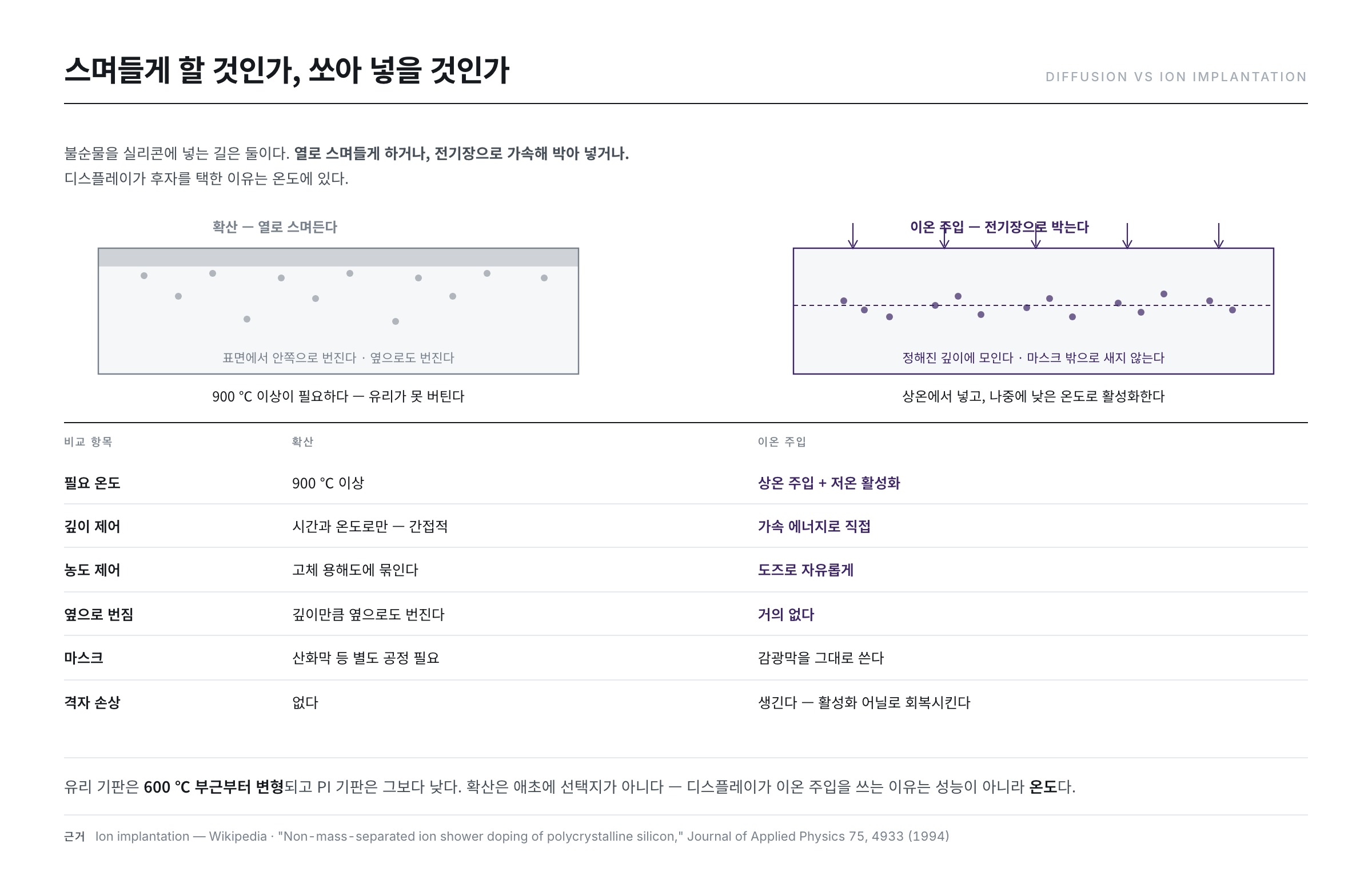
There are broadly two ways to get impurities into silicon.
Diffusion lets them soak in at high temperature under a concentration gradient, exploiting the natural tendency of atoms to move from high concentration to low. The equipment is simple and there is no lattice damage, but the process is isotropic, so the dopant spreads sideways as well, and concentration and depth cannot be set independently. Above all it needs high temperature, which rules it out on glass.
Ion implantation turns the impurity into ions and accelerates them electrically to drive them in by force (Ion implantation). It works at low temperature, lets you set depth with the acceleration energy and concentration with the dose independently, and allows photoresist to serve as the mask. In exchange, the ions batter the lattice and leave damage that has to be recovered by the activation anneal foreshadowed in Part 4.
| Criterion | Diffusion | Ion implantation family |
|---|---|---|
| Process temperature | High — unsuitable for glass | Low temperature possible — implanted near room temperature |
| Depth control | Tied to temperature and time | Set independently by acceleration energy |
| Concentration control | Entangled with depth | Set independently by dose |
| Profile shape | Maximum at the surface, monotonically decreasing | Bell shape with a buried peak (Rp) |
| Lateral spread | Isotropic — spreads sideways | Directional — little lateral spread |
| Masking | Needs a heat-resistant mask such as oxide | Photoresist can be used directly |
| Lattice damage | Essentially none | Yes — activation anneal mandatory |
| Backplane use | Effectively impossible | Standard |
The reason displays choose the implantation family is blunt: glass cannot take the heat. Diffusion is not ruled out by preference but by physics.
Where do the ions stop?
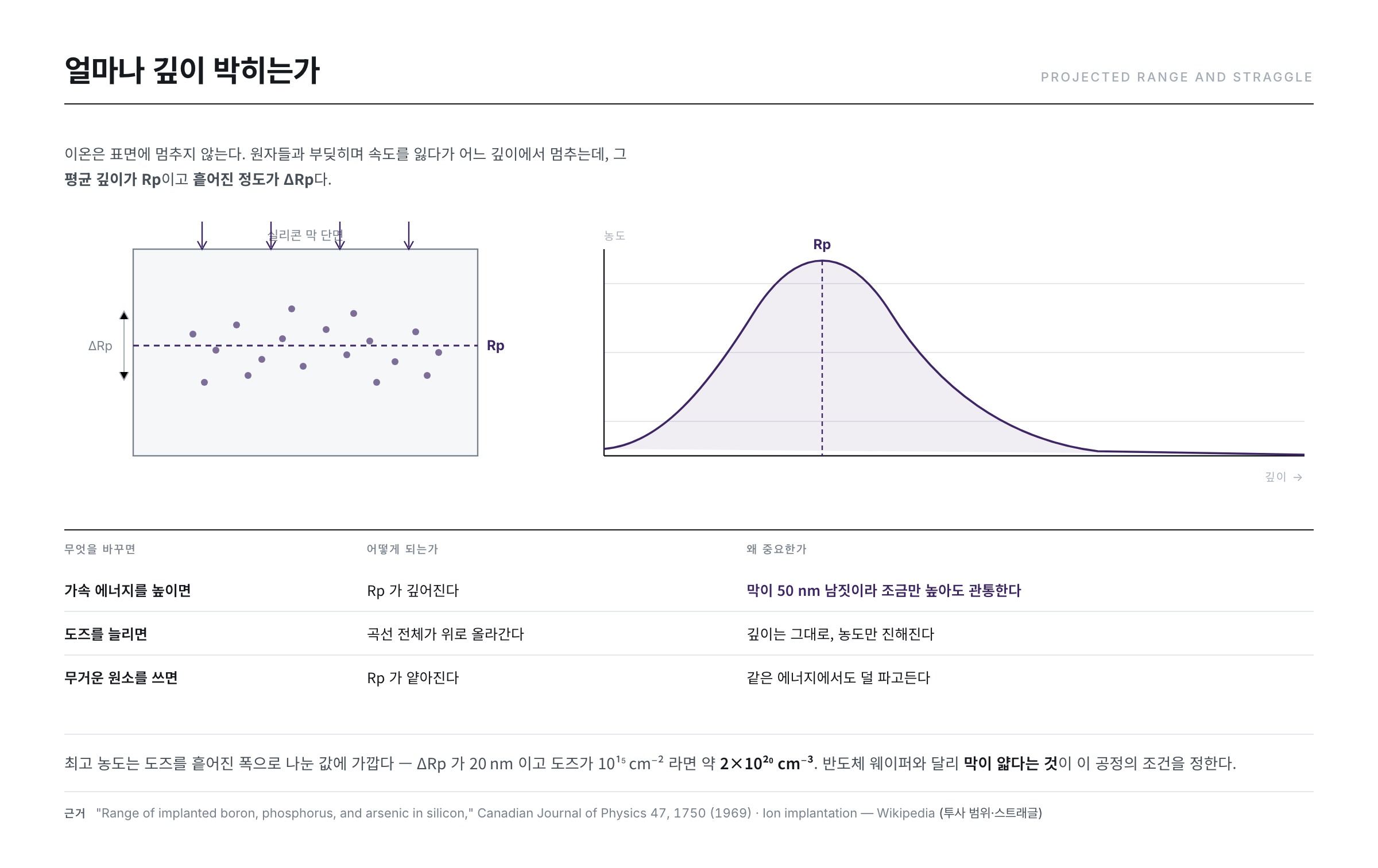
- Implanted ions collide with electrons and atoms inside the silicon, lose energy and eventually stop.
- The distribution of stopping positions is roughly a normal distribution.
- The mean depth is called the projected range (Rp) and its standard deviation ΔRp.
- The heavier the ion, the shallower it stops — and the more damage it does to the lattice.
This distribution was pinned down experimentally as early as the 1960s. The early study that tabulated the range of boron, phosphorus and arsenic implanted into silicon as a function of energy ("Range of implanted boron, phosphorus, and arsenic in silicon," Can. J. Phys. 47, 1750 (1969)) is the root of the range data that today's process simulators inherited.
Two units must be kept apart here. Dose is the number of ions implanted per unit area (cm⁻²); concentration is the number per unit volume (cm⁻³). For the same dose, a shallow pile-up gives a higher concentration and a wide spread gives a lower one. Assuming a normal distribution, the peak concentration follows:
peak concentration = dose ÷ (√(2π) × ΔRp) ≈ dose ÷ (2.507 × ΔRp)
For instance, with ΔRp of 20 nm (2×10⁻⁶ cm), a dose of 1×10¹⁵ cm⁻² peaks at about 2×10²⁰ cm⁻³. Squeeze the same dose into half the thickness and the concentration doubles — which is why acceleration energy and dose cannot be chosen separately if a particular profile is wanted.
There is a trap as well. A crystal lattice contains empty tunnels along the directions in which atoms line up, and an ion that happens to enter along one of them slips through without collisions and buries itself far deeper than expected — channelling. Boron, being light, is especially vulnerable, and measurements show that a change of only a few degrees in incidence angle visibly alters the profile ("Incidence Angle Dependence of Planar Channeling in Boron Ion Implantation into Silicon," J. Electrochem. Soc. 130, 716 (1983)). Tilting the substrate slightly during implantation is therefore standard practice. In polycrystalline silicon, however, each grain has its own orientation, so a single tilt angle cannot eliminate channelling the way it does on a wafer; it only mitigates it on average.
The large-area answer — give up mass separation
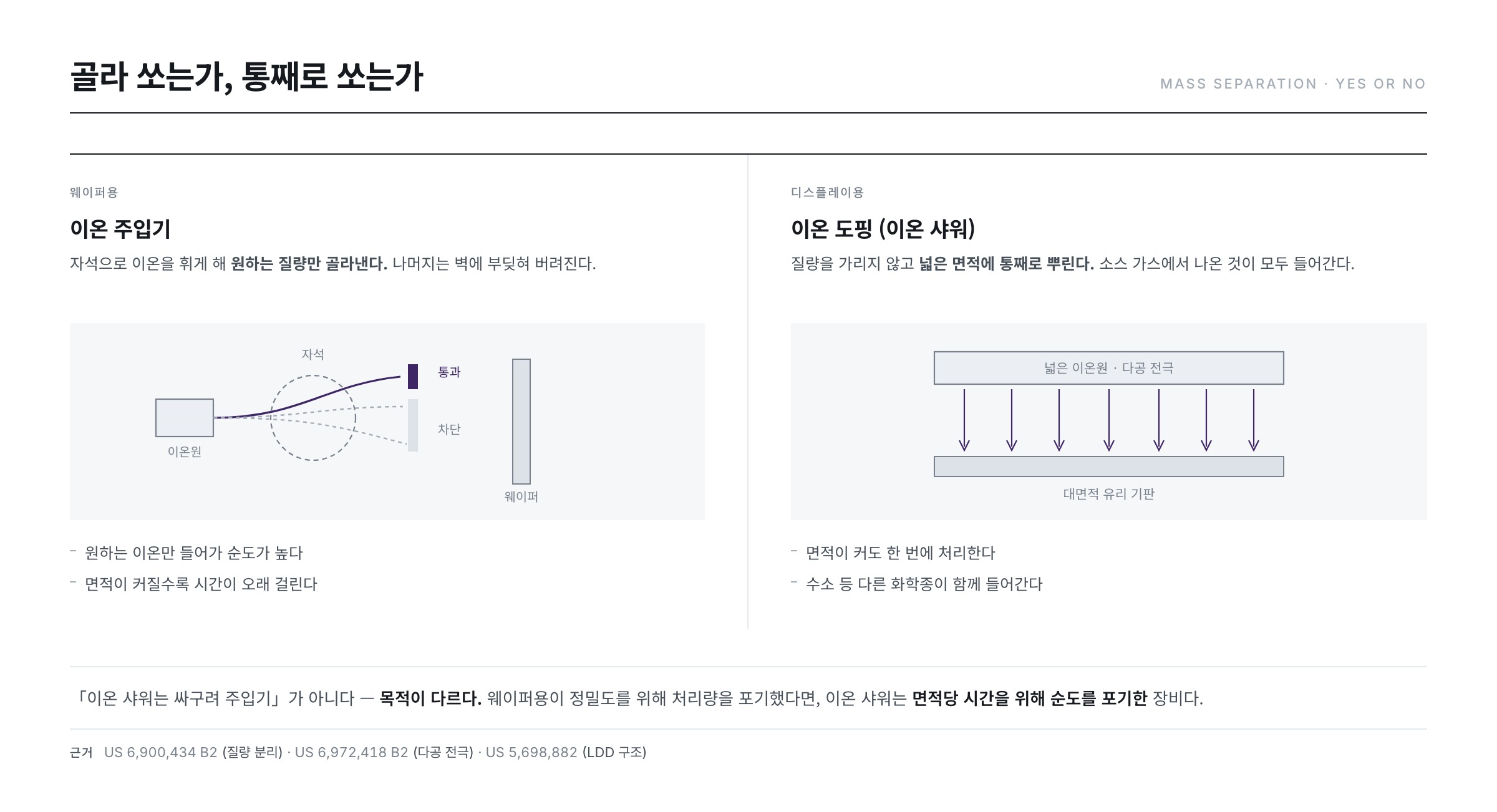
Making the ions works the same way in both cases. In a high-vacuum chamber a filament is heated to emit thermal electrons, magnets confine those electrons, and the source gas (phosphine, PH₃, for phosphorus and diborane, B₂H₆, for boron, both diluted in hydrogen) is ionised into a plasma. The fork in the road comes next.
- Ion implantation (mass-separated) — a magnetic field bends the ions according to mass so that only the wanted species is accelerated. Purity and precision are high, but the beam area is small. This is the standard method for semiconductor wafers.
- Ion doping / ion shower (non-mass-separated) — ions are pulled straight out of the plasma with no separation step and sprayed over a wide area like a shower. The advantage on large glass is overwhelming, which is why it became the mainstream of display manufacturing.
| Criterion | Ion implantation (mass-separated) | Ion doping / ion shower (non-separated) |
|---|---|---|
| Ion selection | Separated by mass in a magnetic field | No separation — the plasma composition arrives as it is |
| Beam form | Narrow precise beam — must be scanned | A shower covering a wide area at once |
| Purity | High — only the wanted ion | Low — hydrogen and compound ions come along |
| Energy uniformity | Single energy | Mixed species spread the effective energy |
| Dose rate / throughput | Low — worse as area grows | High — better as area grows |
| Main stage | Semiconductor wafers | Large-area glass substrates |
The price of abandoning mass separation is purity. The literature is explicit about it: because the ions are not mass-analysed, the flux reaching the substrate contains several species differing in mass, charge and energy, and with B₂H₆ the ions H₂⁺, H₃⁺ and BHₓ⁺ are implanted alongside the intended dopant, causing unintended doping and energy contamination ("Non-mass-separated ion shower doping of polycrystalline silicon," J. Appl. Phys. 75, 4933 (1994)). The method is chosen anyway because of its high dose rate and large-area capability, and the resulting device characteristics are reported to be comparable with conventional implanters.
Equipment development therefore splits into two branches: attempts to restore mass separation even in a wide beam (US 6,900,434 B2 — Method and device for separating ion mass, and ion doping device), and designs that skip separation and instead extract ions evenly over a wide area through an electrode perforated with a dense array of apertures (US 6,972,418 B2 — Ion doping apparatus, and multi-apertured electrode for the same). Redesigning the ion source itself for large areas has also been reported ("Multi-cusp ion source for doping process of flat panel display manufacturing," Rev. Sci. Instrum. 85 (2014)). All of them answer the same question — how do you preserve uniformity as the substrate grows?
There is an interesting side effect here. If hydrogen compound ions come along for the ride, then hydrogen is being put back into the film. The very hydrogen we worked so hard to drive out in Part 4 can, at the doping stage, help by filling dangling bonds at the grain boundaries — which is exactly why the hydrogen budget has to be managed across the whole process flow.
Implantation is always followed by an anneal
Ion implantation wrecks the silicon lattice, because ions arriving at high speed knock atoms off their sites. On top of that, a dopant only works electrically once it sits on a proper substitutional site — wedged in an interstitial gap it releases no carrier and merely acts as a scattering centre that lowers mobility. Solving both problems — lattice recovery and dopant activation — with a single heating step is the activation anneal flagged in Part 4.
The thermal budget problem returns here. If the anneal is too cool or too short, activation is incomplete; too hot or too long and the dopant diffuses, smearing the profile you worked to create. That is exactly why the rapid thermal approach seen in Part 5 is attractive — ramp up and down in a few seconds and you get activation with minimal diffusion.
There is a more extreme option too: using the excimer laser from Part 7 for activation directly. Because it heats only the surface on a nanosecond timescale, almost no heat reaches the glass, and the dopants align onto lattice sites as the film melts and resolidifies ("Study on dopant activation of phosphorous implanted polycrystalline silicon thin films by KrF excimer laser annealing," Solid-State Electronics 46, 1085 (2002)). The catch is that with laser activation, irradiation uniformity acts exactly like dose uniformity, so the energy-density control problem from Parts 6 and 7 is inherited wholesale.
Limits and common misconceptions
- "More doping always means better conduction." — Past a certain point, no. Dopant beyond the solid solubility limit fails to occupy lattice sites and clusters instead, and even activated dopant scatters carriers and lowers mobility. Resistance is set by the product of concentration and mobility, so raising concentration alone gives sharply diminishing returns.
- "The implanted dose equals the active carrier concentration." — It does not. The activation fraction depends on the anneal, and in polycrystalline silicon a substantial share of the dopant is trapped at grain boundaries and contributes nothing electrically. That is why the fab manages the dose and measures sheet resistance.
- "Ion shower is just a cheap implanter." — The goals differ. A wafer implanter trades throughput for precision; an ion shower trades purity for area per unit time.
- "Channel doping makes the channel conductive." — The opposite. Its concentration is three decades below source/drain, and the aim is not to carry current but to move the threshold voltage.
What the fab watches — three control points
- Dose uniformity — the same amount must land everywhere on the substrate. Position-to-position dose differences become threshold-voltage scatter and finally show up as visible mura. The larger the substrate, the more the uniformity of beam scan and substrate transport matters, which is precisely why ion sources and extraction electrodes keep being redesigned.
- Depth profile — stability of the acceleration energy is stability of the junction depth. With a film only about 50 nm thick, a slightly high energy sends the dopant clean through. Tilt control against channelling belongs here too.
- Activation fraction and residual damage — whether the post-implant anneal was sufficient is checked indirectly through sheet resistance. As the earlier table shows, resistance is roughly inversely proportional to concentration, so sheet resistance is a mirror reflecting dose, anneal and activation all at once.
The silicon now carries its polarity. From the next instalment (Part 9) we move into the deposition chapter — what vacuum actually is, why plasma is needed, and how metal wiring and insulating films are stacked one layer at a time on that stage.
References
- "Non-mass-separated ion shower doping of polycrystalline silicon," Journal of Applied Physics 75, 4933 (1994) : species contamination in non-mass-separated ion shower and the resulting device characteristics
- "Multi-cusp ion source for doping process of flat panel display manufacturing," Review of Scientific Instruments 85 (2014) : ion source design for large-area doping
- "Incidence Angle Dependence of Planar Channeling in Boron Ion Implantation into Silicon," Journal of The Electrochemical Society 130, 716 (1983) : incidence angle and channelling — the basis for tilted implantation in the text
- "Range of implanted boron, phosphorus, and arsenic in silicon," Canadian Journal of Physics 47, 1750 (1969) : early measurements of projected range per dopant and energy
- "Study on dopant activation of phosphorous implanted polycrystalline silicon thin films by KrF excimer laser annealing," Solid-State Electronics 46, 1085 (2002) : low-temperature activation using a laser
- "Photo-Leakage Current of Poly-Si Thin Film Transistors with Offset and Lightly Doped Drain Structures," Japanese Journal of Applied Physics 38, 5757 (1999) : LDD and offset structures versus leakage current
- US 6,900,434 B2 — Method and device for separating ion mass, and ion doping device : attempting mass separation in a wide ion beam
- US 6,972,418 B2 — Ion doping apparatus, and multi-apertured electrode for the same : multi-apertured electrode for large-area extraction
- US 5,698,882 — LDD Polysilicon thin-film transistor : a polycrystalline silicon device with an LDD structure
- Doping (semiconductor) — Wikipedia : definitions of donor, acceptor, N-type and P-type
- Ion implantation — Wikipedia : projected range, straggle, channelling, implantation damage and annealing
- Silicon — Wikipedia : density and atomic weight — the basis for the atomic density calculation in the text