In the previous installment we set up the structure of the field-effect transistor. The gate sits on top of an insulating film and does not touch the channel, and yet applying a voltage to the gate turns the surface beneath the film over, creating a channel joining source and drain. The gate voltage at which that channel begins to appear was given the name threshold voltage.
That far is what the gate does. This installment looks at the other half. Once the channel has been made, how does the current change as the drain voltage is raised — and why, past a certain point, does raising it further add nothing?
The answer stated first comes in three pieces. With no channel, nothing flows. With a channel, the current grows as much as you raise it. But past a certain line, raising it further leaves it unchanged. Each of these three stretches has a name and a defining inequality.
The operating values in this text are examples meant to show how a calculation goes, not the specifications of any particular company. Every figure quoted here was confirmed in published literature, and the sources are listed at the end.
Two Inequalities Divide the Three Regions
We deal with two voltages: VGS, between gate and source, and VDS, between drain and source. The three regions are separated entirely by comparing these two once each. What follows is written for the NMOS, in which electrons flow.
The Wikipedia "MOSFET" article states the conditions for the three regions as follows.
- Cut-off — VGS < Vth. No channel has been made. The "MOSFET" article describes this as the transistor being turned off, with no conduction between drain and source.
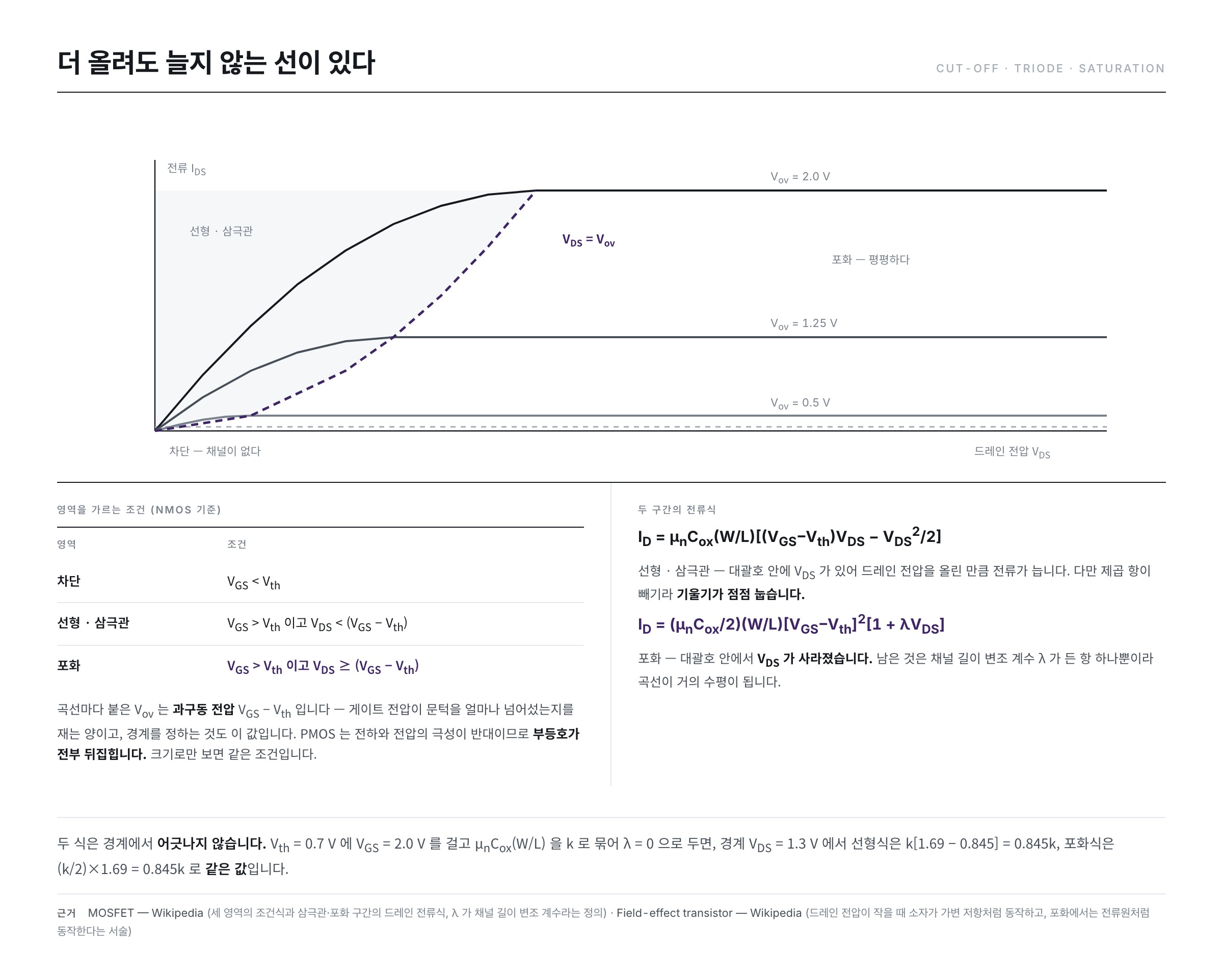
- Triode / linear — VGS > Vth and VDS < (VGS − Vth). The channel runs continuously from source to drain. The "MOSFET" article describes the device in this stretch as a resistor whose value is set by the gate voltage.
- Saturation — VGS > Vth and VDS ≥ (VGS − Vth).
Both inequalities contain the same quantity, VGS − Vth. It measures by how much the gate voltage has crossed the threshold. The "MOSFET" article gives this quantity the name overdrive voltage, Vov. Whenever a boundary is mentioned in this article from here on, this is the value it is measured against.
The Linear Stretch — It Behaves Like a Resistor
The Wikipedia "Field-effect transistor" article explains this stretch as follows. When the drain voltage is much smaller than the gate voltage, changing the gate voltage changes the resistance of the channel, and the drain current is proportional to the drain voltage. The "Field-effect transistor" article states that the device then acts like a variable resistor.
The current equation for this stretch as carried by the "MOSFET" article is as follows.
ID = μn Cox (W / L) [ (VGS − Vth) VDS − VDS2 / 2 ]
Unpacking the symbols one at a time gives this.
- μn — the effective mobility of the carriers. It expresses how fast carriers are pulled along in a given electric field.
- Cox — the capacitance per unit area of the gate insulator. It settles how much charge a given gate voltage can draw into the channel.
- W — the width of the gate. The breadth of the road the current takes.
- L — the length of the gate. The distance to be covered from source to drain.
As seen in the previous installment, the gate insulator is itself a capacitor. Dividing the parallel-plate capacitance C = ε A / d of the Wikipedia "Capacitor" article by the area gives the value per unit area, so Cox is the permittivity of the insulator divided by its thickness. The thinner the insulator, the larger Cox becomes and the more current flows at the same voltage.
It Is Called Linear but Is Not Quite a Straight Line
Looking at the equation, inside the brackets there is one VDS term and one VDS2 term. The latter is subtracted, so as the drain voltage is raised the slope tips over a little at a time. Let us confirm it with numbers.
This article assumes an NMOS with Vth = 0.7 V to which VGS = 2.0 V is applied, and calculates accordingly. We bundle μn Cox (W / L) together and call it k, and set the channel-length modulation coefficient λ, which appears later, to 0. The overdrive voltage is Vov = 2.0 − 0.7 = 1.3 V.
- VDS = 0.1 V → ID = k [ 1.3 × 0.1 − 0.12 / 2 ] = k [ 0.13 − 0.005 ] = 0.125 k
- VDS = 0.2 V → ID = k [ 0.26 − 0.02 ] = 0.240 k
- VDS = 0.4 V → ID = k [ 0.52 − 0.08 ] = 0.440 k
- VDS = 1.3 V → ID = k [ 1.69 − 0.845 ] = 0.845 k
Doubling from 0.1 V to 0.2 V made the current 1.92 times larger. Doubling again from 0.2 V to 0.4 V made it 1.83 times larger this time. Twice as much went in, but less than twice as much came out. And the shortfall keeps growing.
This is why the same stretch carries two names, linear and triode. When the drain voltage is very small the VDS2 term is negligible and the line is nearly straight, and that part is called linear. Raise the drain voltage further and that term grows, the curve tips over, and that part is called triode. The inequality is the same. It is merely a matter of naming the head and the tail of the curve separately.
Why it tips over becomes visible when you look at the shape of the channel. As the drain voltage grows, the channel thins out at the drain end. The Wikipedia "Threshold voltage" article states that when the drain voltage is positive the channel becomes narrower, and explains the reason as being that the voltage dropped across the resistive channel reduces the electric field across the insulator. A road that narrows cannot fail to gain resistance.
The Saturation Stretch — the Channel Is Cut, Yet Current Flows
Keep raising the drain voltage and the thinning channel at the drain end eventually disappears. The "Field-effect transistor" article describes this state as the shape of the inversion region being pinched off at the drain end.
Where It Is Cut Comes Out of a Calculation
What settles whether a channel exists is the voltage between the gate and that point. At a point on the source side that value is VGS. At the drain end, VDS has already been dropped along the way, so what remains is VGS − VDS. This is called the gate-to-drain voltage, VGD.
The channel exists only where this value exceeds the threshold. So the condition at the instant the channel at the drain end is just disappearing is VGD = Vth. Putting the two expressions together,
VGS − VDS = Vth → VDS = VGS − Vth
Out comes the very boundary that divided the regions above. The inequality that separates the regions is not a rule to be memorised but a written record of when the channel is cut. With the values assumed above, that place is VDS = 1.3 V.

Why Current Remains After the Cut
A natural question arises here. If the road is cut, should the current not be cut as well? It is not.
The "Field-effect transistor" article makes this clear. In the saturation stretch, even though the conducting channel made by the gate no longer joins source and drain, the movement of carriers is not thereby blocked. The electrons that made up the channel, when drawn by the drain voltage, can pass through the depletion region and out of the channel. It is the same depletion region seen in the earlier installments — it merely has no carriers of its own to move about; it cannot block what the electric field carries through it.
The "MOSFET" article says the same thing from another angle. Even when the channel does not extend across the whole device, the electric field between drain and channel is very high, so conduction continues.
Why, then, does the current not grow? The "Field-effect transistor" article gives the reason. Raising the drain voltage increases the distance from the drain to the pinch-off point, and the resistance of the depletion region rises by that much. The resistance rises together with the voltage, so the current stays almost unchanged. Because of this proportionality, the device in the saturation stretch behaves not as a resistor but as a current source, and the size of that current is set by the gate voltage.
The Current Equation for the Saturation Stretch
The equation for this stretch as carried by the "MOSFET" article is as follows.
ID = (μn Cox / 2) (W / L) [ VGS − Vth ]2 [ 1 + λ VDS ]
Compared with the previous equation, VDS has vanished from inside the brackets. All that remains is the trailing [ 1 + λ VDS ], and the "MOSFET" article calls λ the channel-length modulation coefficient, explaining that this term is precisely what carries the share by which the pinch-off point shifts with the drain voltage. If λ is small, the curve is nearly horizontal.
Let us check that the two equations do not disagree at the boundary. Keeping the earlier assumptions, Vov = 1.3 V and λ = 0.
- Putting VDS = 1.3 V into the linear equation → k [ 1.69 − 0.845 ] = 0.845 k
- Putting it into the saturation equation → (k / 2) × 1.32 = (k / 2) × 1.69 = 0.845 k
The same value. They are two different equations, yet they meet exactly at the boundary. The curve does not break; rather, its character changes at the vertex of one and the same curve.
To add a note, the current in the cut-off stretch is not strictly 0 either. The "MOSFET" article writes the subthreshold current as ID ≈ ID0 e(VGS − Vth) / nVT. It is the same shape as the diode equation of an earlier installment, and VT is the same thermal voltage — the value the Wikipedia "Boltzmann constant" article records as about 25.85 mV at 300 K. Even while you believe the switch is off, a very small current is leaking along an exponential.
NMOS and PMOS — Flipping the Signs
Everything so far has been the NMOS, in which electrons flow. The PMOS, in which holes flow, repeats the same story with only the signs flipped.
The "MOSFET" article distinguishes the structures of the two as follows. In an n-channel device the source and drain are n+ and the body is p-type; in a p-channel device the source and drain are p+ and the body is n-type. The carriers that cross the channel are electrons for the n-channel and holes for the p-channel.
The direction of the voltages flips as well. The "MOSFET" article states that applying a negative gate-to-source voltage creates a p-channel at the surface of the n region, and that this is the same story as the n-channel case with only the polarity of charge and voltage reversed. And it describes how, when the gate voltage is less negative than the threshold, the channel vanishes and only a very small subthreshold current remains.
The inequalities set up above therefore all reverse direction for the PMOS. The condition for turning it on is VGS < Vth (Vth itself being negative), and the condition for entering saturation is VDS ≤ VGS − Vth. In magnitude alone they are exactly the same as for the NMOS. The difference is whether a sign is attached or removed.
At the Same Size, a PMOS Delivers Less Current
There is one place, however, where the symmetry is not complete: mobility.
Let us bring back the values seen in the first installment of this series. The table in the Wikipedia "Electron mobility" article records the mobilities in crystalline silicon as follows.
- electrons 1,400 cm2/(V·s)
- holes 450 cm2/(V·s)
The μ standing at the head of the current equation is precisely this value. Keep the other conditions — W, L, Cox, the overdrive voltage — all the same, and the ratio of currents is just the ratio of mobilities.
450 ÷ 1,400 ≈ 0.32
A PMOS built to the same size can deliver only about 1/3 of the current of an NMOS. Conversely, to make it deliver the same current, the width W must be widened by 1,400 ÷ 450 ≈ 3.1 times.
Explaining a switch that uses the two devices side by side, the "MOSFET" article states that the pMOS is made two to three times wider than the nMOS. Only then do the speeds in the two directions match. It is a number in the same range as the 3.1 times that came out of the mobility ratio.
The "MOSFET" article sums up the reason in a single sentence as well. If the current-delivering capability is to be equal, the n-channel device can be made smaller than the p-channel device, because holes, the carriers of the p-channel, have lower mobility than electrons, the carriers of the n-channel.

In sum, the PMOS is the NMOS reflected in a mirror, but the mirror is not perfectly flat. The physics is symmetric; the material is not. When, in later installments dealing with circuits, you see a drawing in which the two devices differ in size, that is not a designer's taste but the work of the two numbers in this table.
Summary
- The regions are separated by two comparisons. Compare VGS with Vth to see whether a channel exists, and compare VDS with VGS − Vth to see whether that channel runs all the way through.
- In the linear/triode stretch the device is a resistor whose value is set by the gate voltage. Because the equation has a VDS2 term it is not quite a straight line despite the name — put in twice as much and 1.9 times comes out; put in twice as much again and 1.8 times comes out.
- The boundary VDS = VGS − Vth is not a rule to be memorised but VGD = Vth rewritten. It is the place where the channel at the drain end disappears.
- Even when the channel is cut, the current is not. Carriers cross the depletion region carried by the electric field. Raise the drain voltage and the resistance of that stretch rises with it, leaving the current almost constant.
- The PMOS is an NMOS with the signs flipped. But the mobility of holes is lower, 450 against 1,400, so at the same size the current is about 1/3.
Up to here is the story of a single transistor behaving ideally. The next installment looks at the point where that ideal breaks down — where the above equations begin to fail once a device is made small and the channel becomes short.
References
- MOSFET — Wikipedia : the conditions for the three operating regions (cut-off VGS < Vth, triode VGS > Vth and VDS < VGS − Vth, saturation VDS ≥ VGS − Vth), the current equations for the two stretches and the definitions of μn, Cox, W, L and λ, the overdrive voltage, the subthreshold exponential current equation, the statement that conduction continues even at pinch-off because the field is high, the source, drain and body composition of the n/p channels and the reversal of polarity, the statement that the pMOS is made two to three times wider than the nMOS, the statement that because the mobility of holes is lower the n-channel can be made smaller for the same drive
- Field-effect transistor — Wikipedia : the statement that it acts like a variable resistor when the drain voltage is small, the statement that the inversion region is pinched off at the drain end, the explanation that in saturation carriers still move through the depletion region and that raising the drain voltage raises both the distance to the pinch-off point and the resistance so that the current is held constant, the statement that the device in the saturation stretch acts like a current source
- Threshold voltage — Wikipedia : the definition of the threshold voltage (the minimum gate-to-source voltage that creates a conducting path joining source and drain), the statement that the channel becomes narrower when the drain voltage is positive
- Electron mobility — Wikipedia : the mobilities in crystalline silicon — electrons 1,400 cm2/(V·s), holes 450 cm2/(V·s)
- Capacitor — Wikipedia : the parallel-plate capacitor C = ε A / d
- Boltzmann constant — Wikipedia : the thermal voltage VT = kT / q, about 25.85 mV at 300 K
- ※ The portions quoted above from Wikipedia articles are licensed under CC BY-SA 4.0.