With the stage of vacuum and plasma ready (Part 9), it is time to actually build films on it. The films that go onto a backplane fall into two groups — metals that conduct and insulators that do not. This instalment covers the metals, through sputtering. Gate wiring, source/drain wiring and pixel electrodes are all made this way.
Two branches of deposition — physical or chemical
There are two ways to build a thin film, divided by principle.
- PVD (physical vapour deposition) — the material is removed and transported by physical force. It moves as it is, with no chemical reaction. Evaporation and sputtering belong here.
- CVD (chemical vapour deposition) — gases are made to react chemically and the product is deposited on the surface. That is the subject of the next part.
The simplest PVD method is evaporation. Material is placed in a boat of a refractory metal such as tungsten or molybdenum, current is passed to heat it, and the material vaporises and sticks to the substrate above. It proceeds in four steps: phase change, transport, adsorption, surface rearrangement. High-melting-point materials may instead be heated by an electron beam — fast, capable of refractory materials, but with the burden of possible X-ray generation.
| Method | Force that removes material | Operating pressure | Energy of arriving atoms | Suitability for large area |
|---|---|---|---|---|
| Resistive evaporation | Heat — melt and vaporise | below 10⁻⁵ Torr | about 0.1 eV | Low — point source, shadowing |
| Electron beam evaporation | Local heating by an electron beam | below 10⁻⁵ Torr | about 0.1–0.2 eV | Low to medium |
| Magnetron sputtering | Ion momentum transfer | 1–10 mTorr | a few eV | High — wide planar target |
The rightmost column is the conclusion. Evaporation is by nature a point-source process, so edges thin out as the substrate grows, and as Part 9 showed, λ reaches 50 m in the 10⁻⁶ Torr band, making transport perfectly line-of-sight and shadowing severe. The workhorse of large-area displays is therefore sputtering.
Knocked loose — the principle of sputtering
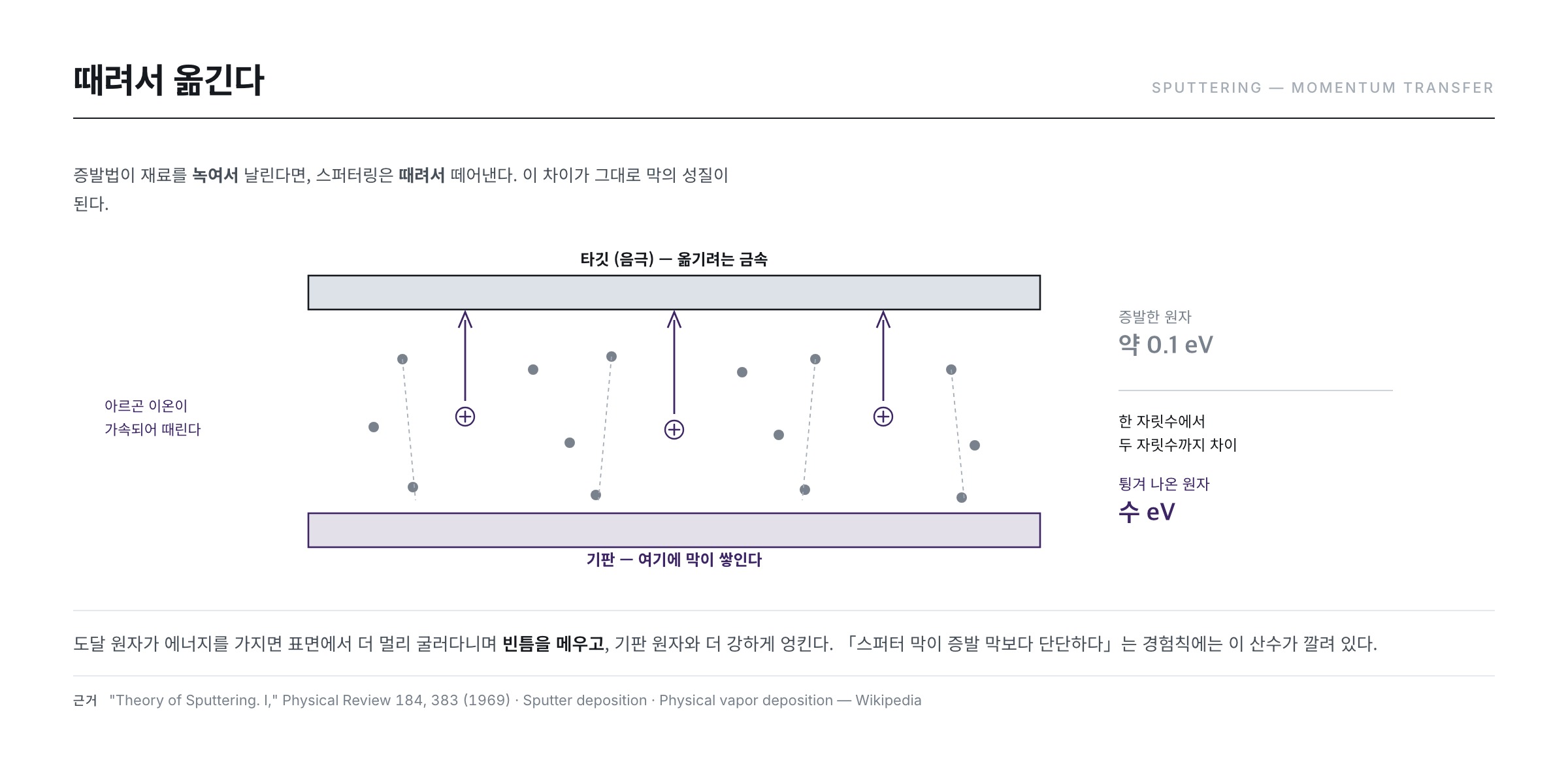
Sputtering is closer to billiards. An inert gas such as argon is fed into the vacuum chamber and a plasma is struck, producing Ar⁺ ions. The metal to be deposited (the target) is placed at the cathode, and the electric field accelerates the ions towards it. An ion arriving at high speed collides with a target atom and transfers momentum, so the atom is ejected from the surface and lands on the substrate opposite (Sputter deposition).
Numbers reveal the character of the process. Removing a single metal atom from the surface takes on the order of a few eV, whereas the incoming ion carries far more — tens to hundreds of eV. Because it strikes with energy to spare, material can be transported regardless of melting point, which is the decisive difference from evaporation, where the material must be melted.
How many atoms one ion knocks loose is the sputter yield. What determines it was worked out theoretically in the 1960s: the incoming ion creates a collision cascade inside the target, some of which returns to the near-surface region and pushes atoms out, and the yield follows from the incident energy, the mass ratio of ion to target, and the surface binding energy of the target ("Theory of Sputtering. I. Sputtering Yield of Amorphous and Polycrystalline Targets," Phys. Rev. 184, 383 (1969)). This is also why argon became the standard sputter gas — chemically inert, similar in mass to the main wiring metals so momentum transfer is efficient, and inexpensive.
Ion bombardment does not only cause sputtering. Ions may be reflected, secondary electrons may be emitted, ions may embed themselves in the surface, and underlying layers may be damaged. The sputter process is the art of using only the ejection of atoms out of all these effects.
Why sputtered films adhere better
This is why the table compared the energy of arriving atoms. In evaporation, that energy is set by the source temperature. An atom vaporised at 1,500 K carries thermal energy of
kT = 1.381×10⁻²³ × 1,500 ÷ 1.602×10⁻¹⁹ ≈ 0.13 eV
and no more. A sputtered atom, by contrast, has overcome the surface binding energy and carries several eV — one to two orders of magnitude more. That energy difference becomes the film's character. Arriving atoms can move further across the surface, filling gaps and interlocking more strongly with substrate atoms, so adhesion and density improve. The fab rule of thumb that "sputtered films are tougher than evaporated ones" rests on this arithmetic.
One magnet changed the game — the magnetron
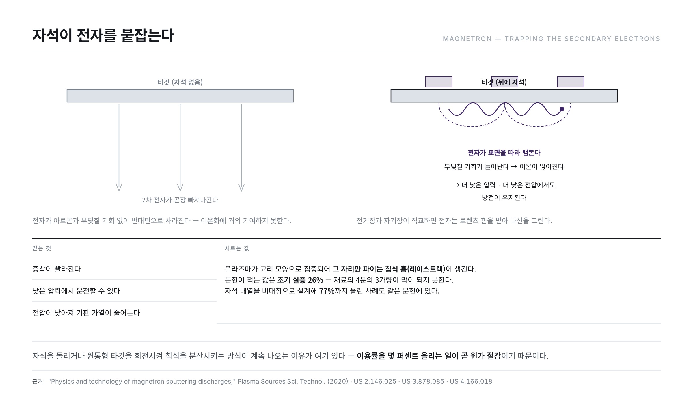
Early DC sputtering had a decisive inefficiency. The secondary electrons needed to sustain the plasma escaped straight across from the target and contributed almost nothing to ionising the gas.
The solution was a magnet. Placing magnets behind the target creates a magnetic field parallel to the target surface; electric and magnetic fields cross, and the electrons follow spiral paths under the Lorentz force, unable to leave the neighbourhood of the target.
The idea itself is old. A configuration that applies a magnetic field to the discharge space to lengthen electron paths, and uses the sustained discharge to knock material off the cathode onto a substrate, is described in patents from the 1930s (US 2,146,025 — Coating by cathode disintegration). What changed the industry, however, was the planar magnetron. Once the arrangement of magnets behind a wide plate-shaped target — forming a closed magnetic tunnel along the surface — was set out in the 1970s (US 3,878,085 — Cathode sputtering apparatus, US 4,166,018 — Sputtering process and apparatus), today's method of covering a large area in one pass became possible.
The result is dramatic. The literature puts it this way: "the main purpose of the magnetic field arrangement is to confine electrons and increase their residence time near the target, which allows the discharge to be sustained at lower pressure and lower discharge voltage." And this intense ion bombardment removes target atoms at a far higher rate than without magnetic confinement, so deposition speeds up ("Physics and technology of magnetron sputtering discharges," Plasma Sources Sci. Technol. (2020)).
The side effects are welcome too — operation at lower pressure, a lower applied voltage that reduces substrate heating, and less material landing on chamber walls.
Nothing is free — the racetrack
The price is that the target does not erode evenly. Because the plasma concentrates in a ring following the magnetic field, an erosion groove — the race track — forms at that spot alone. As erosion deepens the field shape changes and the groove sharpens further, so the target must be replaced without ever being fully consumed. The literature reports target utilisation of only 10–20% for a conventional magnetron.
That number is not trivial. It means 80–90% of the target material goes to reclaim and recycling without ever becoming film, and that material cost and replacement downtime rise accordingly. This is why schemes that rotate or move the magnets to spread the erosion, or that rotate a cylindrical target so its whole surface is used, keep appearing. Raising utilisation by a few percentage points is a direct cost reduction.
Branches of power delivery — DC, RF and pulsed
Even with the same magnetron, the character changes with how power is applied.
DC sputtering has one limit: it cannot be used when the target is an insulator. Continuous ion bombardment builds up positive charge on the insulating surface, and that charge repels the following ions until the discharge stops. The solution is the RF discharge from Part 9. At 13.56 MHz the voltage polarity keeps reversing, so charge never has time to accumulate, and insulating materials such as oxides and nitrides can be sputtered.
| Power scheme | Usable targets | Deposition rate | Strength | Weakness |
|---|---|---|---|---|
| DC magnetron | Metals (conductors) only | Fast | Simple hardware and supply; easy to scale up | No insulating targets; arcing in reactive processes |
| RF magnetron | Conductors + insulators | Slow | Oxide and nitride targets possible | Needs a matching network; lower power efficiency; standing waves on large electrodes |
| Pulsed DC | Conductors, and reactive processes forming thin insulating layers | Fast | Periodic polarity reversal sheds accumulated charge — suppresses arcing | More control variables |
| Reactive sputtering | Metal target + reactive gas (O₂, N₂) | Condition dependent | Oxide and nitride films from a metal target | A target poisoning regime where the target surface is contaminated |
Note the "standing waves on large electrodes" entry for RF. The free-space wavelength at 13.56 MHz is about 22 m, and shorter inside a medium. Once electrodes reach the multi-metre class, the voltage on the electrode begins to vary with position and the deposition rate at the centre diverges from that at the edge. This is one practical reason large-area tools favour DC or pulsed DC.
Pressure decides the structure of the film
Even with the same material on the same tool, film character changes with substrate temperature and operating pressure. A classic study organised sputtered film structure in terms of these two variables ("Influence of apparatus geometry and deposition conditions on the structure and topography of thick sputtered coatings," J. Vac. Sci. Technol. 11, 666 (1974)). The gist:
- At higher pressure — as the table in Part 9 shows, λ shortens, so sputtered atoms collide repeatedly and arrive having lost energy. With no energy left to move across the surface, the film grows as a porous columnar structure with voids between columns: low density, and prone to tensile stress.
- At lower pressure — atoms arrive with their energy intact, and reflected neutral argon also hammers the film. Atoms are driven into interstitial positions, giving a film that is dense but in compressive stress.
This is where stress matters. The internal stress of a deposited film can flip in sign from tensile to compressive with only a small change in pressure, as measured and reported for magnetron-sputtered metal films ("Internal stresses in metallic films deposited by cylindrical magnetron sputtering," Thin Solid Films 64, 111 (1979)). High stress bows the substrate (the same bow seen in Parts 2 and 3) and, in severe cases, peels or cracks the film. Fab recipes are therefore a compromise between "deposit fast" and "keep stress near zero" — raising the pressure moves stress towards tension and lowering it towards compression, so the standard approach is to sit near the point where the sign changes.
Why metals are stacked in several layers

The metal layers of a real backplane are not a single film. To see why, you first need a feel for how large the wiring resistance is. Taking a line 5 μm wide and 300 nm thick running for 1 m, and computing R = ρ × length ÷ (width × thickness):
| Material | Resistivity ρ (Ω·m) | Sheet resistance (Ω/sq at 300 nm) | Resistance of a 1 m line (5 μm wide) | Role |
|---|---|---|---|---|
| Copper (Cu) | 1.7×10⁻⁸ | 0.056 | about 11 kΩ | Low-resistance main layer |
| Aluminium (Al) | 2.7×10⁻⁸ | 0.088 | about 18 kΩ | Low-resistance main layer |
| Molybdenum (Mo) | 5.3×10⁻⁸ | 0.18 | about 36 kΩ | Barrier / contact layer |
| Titanium (Ti) | 4.2×10⁻⁷ | 1.4 | about 280 kΩ | Adhesion / barrier layer |
| Transparent conducting oxide | order of 10⁻⁶ | a few Ω | about 1 MΩ | Transparent electrode |
These resistivities are bulk values; real thin films read higher because of grain-boundary and surface scattering. Even so, the relationship between the orders of magnitude holds — build a line out of barrier metal alone and the resistance is two to twenty times that of the main layer; build a signal line out of transparent conducting oxide and it rises by two decades. The longer the line, the more this resistance blunts the signal arriving at the pixel, which shows up as one side of the panel appearing darker.
So instead of demanding low resistance and chemical stability from a single material, the roles are divided between layers.
| Wiring | Construction | What each layer does |
|---|---|---|
| Gate wiring | Relatively simple | Must survive several later high-temperature steps, so heat resistance and stability come first |
| Source/drain wiring | Three-layer sandwich | Middle = low-resistance main layer / bottom = diffusion barrier and adhesion / top = surface protection and contact stability |
| Pixel electrode (OLED) | Transparent oxide / reflective metal / transparent oxide | The middle metal reflects light; the face meeting the organic layer provides a work function suited to charge injection |
Low-resistance metals tend to be soft, diffuse readily into neighbouring layers, and can grow surface hillocks at high temperature. Wrapping them top and bottom in harder metal suppresses all of these at once (Electrical resistivity and conductivity). The pixel electrode has a more complicated brief: reflectance and work function are different physical properties, so one material rarely satisfies both (Work function), and the transparent conducting oxide itself varies greatly in resistivity and transmittance with composition and process, which has kept it a subject of continual improvement ("Present status of transparent conducting oxide thin-film development for Indium-Tin-Oxide (ITO) substitutes," Thin Solid Films 516, 5822 (2008)).
Why this structure matters resurfaces in the etching chapter (Parts 14–16) — three metal layers have to be cut in a single step, and because each layer has different chemistry, etchant design becomes a delicate problem.
Limits and common misconceptions
- "Sputtering melts the material to move it." — No. Melting belongs to evaporation; sputtering knocks atoms out by momentum. That is why very high melting point metals, and alloys, can be transported with composition largely preserved.
- "Higher vacuum always gives a better film." — Sputtering is the exception. Argon is needed to sustain the plasma, so the pressure is raised back into the mTorr band for operation. The base pressure before that should still be low — but that is an indicator of how much residual moisture and oxygen were removed, not the process pressure.
- "A target is used until it is gone." — As seen above, utilisation stops at 10–20%. Most of the rest is recovered and recycled.
- "Deposition rate is proportional to power." — Broadly yes, but not without limit. More power heats the target, increases arcing in reactive processes, and raises the heat load on the substrate. What the glass and the organic films on it can tolerate sets the ceiling.
What the fab watches — three control points
- Thickness and uniformity — wiring resistance is picture quality. As the table shows, resistance is inversely proportional to thickness, so a 10% thinner film reads 11% higher in resistance. A thickness tilt across a large substrate turns into one side of the screen appearing darker.
- Film stress — deposited films carry compressive or tensile stress. High stress bows the substrate or peels the film. Tuning stress with pressure, power and temperature is part of the recipe, and stress is tracked through substrate curvature measurement.
- Target condition and particles — as target erosion progresses, the magnetic field and plasma shape change, and deposition rate and uniformity shift with them. Target life is therefore managed by cumulative energy delivered, not by elapsed time. Deposits accumulating on chamber walls also flake off as particles, so shield replacement and chamber cleaning intervals are essential.
The metal wiring is in place. In the next instalment (Part 11) we move to the other half — the chemistry of building insulating films by PECVD: how silane gas is broken up inside a plasma to become silicon oxide and nitride, and what the quality of those films is judged by.
References
- "Theory of Sputtering. I. Sputtering Yield of Amorphous and Polycrystalline Targets," Physical Review 184, 383 (1969) : sputter yield explained by the collision cascade
- "Physics and technology of magnetron sputtering discharges," Plasma Sources Science and Technology (2020) : magnetic electron confinement, low-pressure and low-voltage operation, racetrack erosion and 10–20% target utilisation
- "Influence of apparatus geometry and deposition conditions on the structure and topography of thick sputtered coatings," Journal of Vacuum Science and Technology 11, 666 (1974) : the relation between pressure, substrate temperature and film structure
- "Internal stresses in metallic films deposited by cylindrical magnetron sputtering," Thin Solid Films 64, 111 (1979) : internal stress of sputtered metal films and its pressure dependence
- "Present status of transparent conducting oxide thin-film development for Indium-Tin-Oxide (ITO) substitutes," Thin Solid Films 516, 5822 (2008) : resistivity and transmittance of transparent conducting oxides and directions for improvement
- US 2,146,025 — Coating by cathode disintegration : an early configuration sustaining a discharge with a magnetic field to coat from the cathode
- US 3,878,085 — Cathode sputtering apparatus : planar cathode and magnetic field arrangement
- US 4,166,018 — Sputtering process and apparatus : process and apparatus of the planar magnetron
- Sputter deposition — Wikipedia : the principle of sputtering and momentum transfer
- Physical vapor deposition — Wikipedia : PVD in general and evaporation
- Electrical resistivity and conductivity — Wikipedia : resistivity of metals — the basis of the wiring resistance calculation in the text
- Work function — Wikipedia : electrode work function and charge injection