In the previous part we built the metal wiring. This instalment covers the other half — the films that must not conduct, the insulators. The film separating gate from channel, the films that hold wiring layers apart, and the films that block moisture all belong here. These are made not by sputtering but by chemical reaction.
From physics to chemistry — CVD
CVD (chemical vapour deposition) feeds reactant gases into a chamber, drives a chemical reaction, and deposits the product on the substrate surface. If sputtering is a physical removal that "takes material and carries it", CVD is a chemical construction that "synthesises the material on site" (Chemical vapor deposition).
The problem is how to drive the reaction. Breaking gas molecules apart takes energy, and heat alone would require several hundred to nearly 1000 °C. Glass substrates cannot take that (the temperature ceiling seen in Parts 4 and 5). Display processes therefore use PECVD (plasma-enhanced CVD).
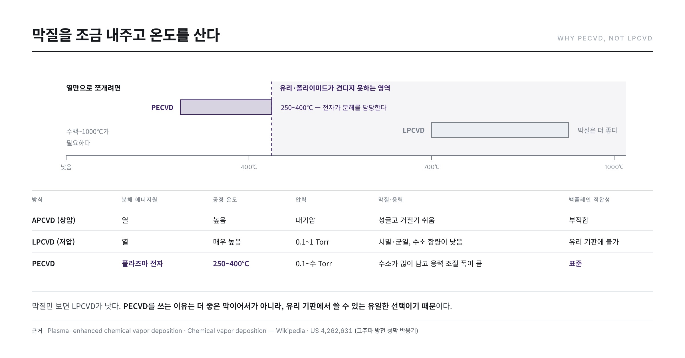
The principle is exactly what Part 9 described. Applying high-frequency power between two electrodes creates a plasma, and electrons accelerated in the field collide with the reactant gas and take over dissociation in place of heat. Films can therefore be grown at a low temperature of roughly 250–400 °C — PECVD deposits at lower temperature than thermal CVD, which makes it useful for temperature-sensitive substrates (Plasma-enhanced chemical vapor deposition). A reactor arrangement that strikes a high-frequency discharge between parallel electrodes and grows films inside it was already set out in patent form around 1980 (US 4,262,631 — Thin film deposition apparatus using an RF glow discharge).
| Method | Source of dissociation energy | Process temperature | Pressure | Film quality and stress | Backplane suitability |
|---|---|---|---|---|---|
| APCVD (atmospheric) | Heat | High | Atmospheric | Tends to be porous and rough | Unsuitable |
| LPCVD (low pressure) | Heat | Very high | 0.1–1 Torr | Dense and uniform, low hydrogen content | Impossible on glass |
| PECVD | Plasma electrons | 250–400 °C | 0.1 to a few Torr | More residual hydrogen; wide stress tuning range | Standard |
The middle column is the whole story. On film quality alone LPCVD is the better choice — thorough thermal reaction leaves less hydrogen and gives more uniform composition. But that "thorough heat" destroys the glass and the polyimide on it. PECVD is a trade that gives up a little film quality to buy temperature, and in backplane processing there is no alternative.
How silane breaks apart
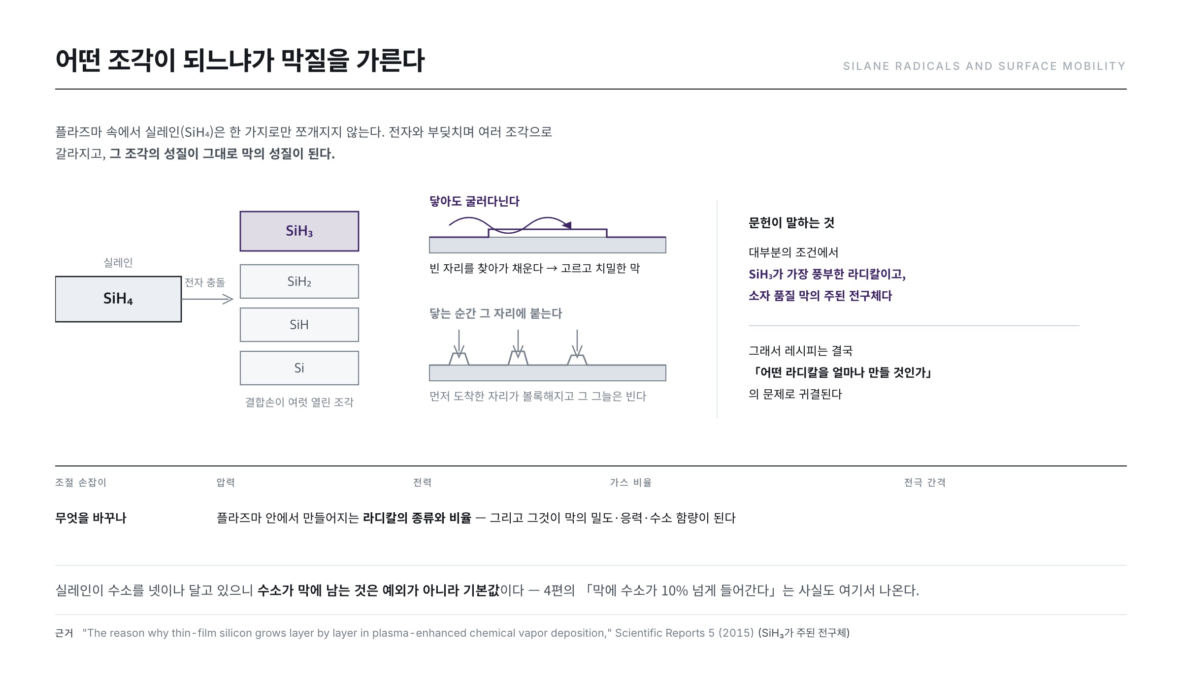
The starting material for display insulators is usually silane (SiH₄). Add an oxygen source (N₂O and the like) and it becomes silicon oxide; add a nitrogen source (NH₃, N₂) and it becomes silicon nitride.
Inside the plasma, silane does not break apart in only one way. Collisions with electrons split it into various fragments (radicals) such as SiH₃, SiH₂, SiH and Si, which reach the surface and form the film. And here is the important fact — which radical dominates decides the quality of the film.
The research literature is explicit. Under most experimental conditions SiH₃ is the most abundant radical in the plasma and the main precursor for "device-quality" films. It is also confirmed that electron-impact dissociation of silane yields mainly the silylene (SiH₂) and silyl (SiH₃) radicals ("The reason why thin-film silicon grows layer by layer in plasma-enhanced chemical vapor deposition," Scientific Reports 5 (2015)).
Why is SiH₃ the good precursor? Because radicals differ in how readily they stick. SiH₂ and bare Si, with several open bonds, attach the instant they touch the surface. Unable to move on from where they landed, the first arrivals build bumps and leave the shadows empty — a porous, rough film. SiH₃, with only one open bond, does not stick easily; it bounces several times and wanders until it finds a site with an available bond. The layer therefore grows evenly, one layer at a time. Both step coverage and film density ultimately come down to this question of "how far can it move on the surface?".
PECVD recipe development therefore reduces to which radicals to make, and how many — with pressure, power, gas ratio and electrode gap as the control knobs. The fact from Part 4 that "more than 10% hydrogen ends up in the film" comes from here too. Silane carries four hydrogens, so what cannot be stripped away stays in the film. This is not a new discovery: it was already measured quantitatively for plasma-deposited nitride in the 1970s ("The hydrogen content of plasma-deposited silicon nitride," J. Appl. Phys. 49, 2473 (1978)).
Why 13.56 MHz?
The specification sheet of almost any PECVD tool lists a frequency of 13.56 MHz. Not because that value is physically optimal, but because it sits in a band internationally reserved for industrial, scientific and medical use. Equipment driving high RF power inevitably leaks electromagnetic radiation, and using this band avoids intruding on communication frequencies, which sharply reduces the regulatory burden.
That said, the choice of frequency does affect the process. Raising the frequency, at the same power, increases plasma density while lowering the energy with which ions strike the substrate. This favours films sensitive to damage, but it also weakens the densifying effect of ion bombardment. Hence dual-frequency drive, applying a low and a high frequency together to tune density and bombardment separately — the same idea seen in part 9, of controlling plasma density and ion energy independently, reappearing here.
Oxide versus nitride — what differs
The two films, made on the same tool by changing only the gas, behave quite differently.
| Property | Silicon oxide (SiOx) | Silicon nitride (SiNx) |
|---|---|---|
| Typical refractive index | about 1.46 | about 1.8–2.0 (varies with composition) |
| Relative permittivity (typical) | about 3.9 | about 7 |
| Blocking of moisture and impurities | Moderate | Excellent — dense network |
| Interface quality | Good — few defects at the silicon interface | Relatively poorer; high hydrogen content |
| Main uses | Buffer, gate insulator, interlayer dielectric | Barrier, encapsulation, some gate insulators |
The permittivity difference enters transistor design directly. The capacitance per unit area of the gate insulator is:
C = ε₀ × relative permittivity ÷ thickness (ε₀ = 8.854×10⁻¹² F/m)
Fixing the thickness at 100 nm gives about 34.5 nF/cm² for oxide and about 62 nF/cm² for nitride. Transistor current is proportional to this capacitance, so nitride yields 1.8 times the drive at the same thickness. Turned around, for the same capacitance nitride can be made as thick as about 180 nm, and a thicker film is correspondingly more robust against pinhole failures. Devices using nitride as the gate insulator of a polycrystalline silicon transistor have indeed been reported ("A high-performance polycrystalline silicon thin film transistor with a silicon nitride gate insulator," IEEE Trans. Electron Devices 45, 2548 (1998)), and the approach of using a high-refractive-index — that is, silicon-rich — nitride at the gate has also been studied ("ZnO-based thin film transistors having high refractive index silicon nitride gate," Appl. Phys. Lett. 91 (2007)).
Oxide nevertheless remains the default gate insulator because of the interface. Electrons in the channel travel within a few nanometres of the insulator, so a defective interface traps and releases them and the threshold voltage wanders. Capacitance can be compensated with thickness; interface quality cannot be compensated at all.
Same tool, different films
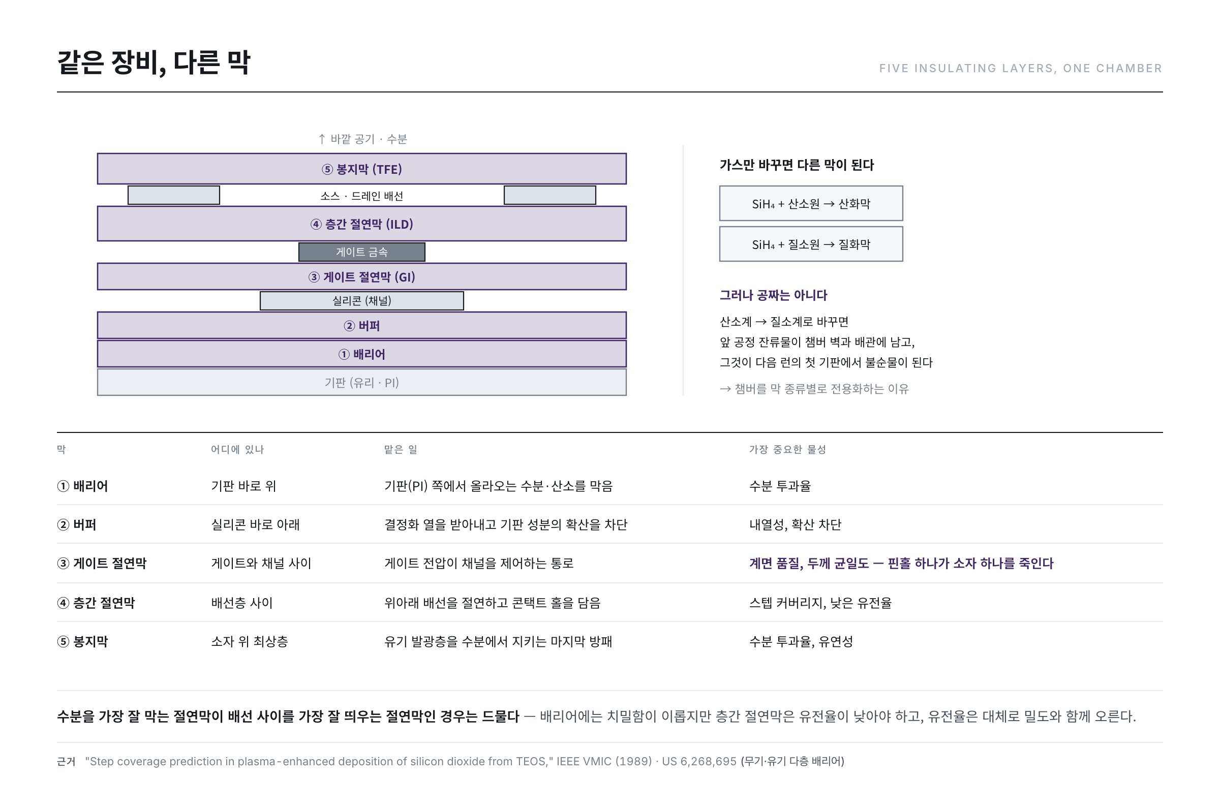
What is interesting is that the same PECVD tool produces films of completely different character. Change the gas and oxide and nitride can be stacked alternately.
| Film | Where it sits | What it does | Most critical property |
|---|---|---|---|
| Barrier | Directly on the substrate | Blocks moisture and oxygen coming up from the polyimide substrate | Water vapour transmission rate |
| Buffer | Directly beneath the silicon | Absorbs crystallisation heat and blocks diffusion of substrate species | Heat resistance, diffusion blocking |
| Gate insulator (GI) | Between gate and channel | The path through which gate voltage controls the channel | Interface quality and thickness uniformity — one pinhole kills one device |
| Interlayer dielectric (ILD) | Between wiring layers | Insulates upper from lower wiring and hosts the contact holes | Step coverage, low permittivity |
| Thin-film encapsulation (TFE) | Topmost layer over the device | The final shield protecting the organic emitting layer from moisture | Water vapour transmission rate, flexibility |
Covering a step — step coverage
Depositing on a flat surface is easy. What is hard is covering an already patterned, uneven surface evenly. If an insulator crossing over wiring thins at the corner, insulation breaks down at that spot. This capability is called step coverage.
Material choice matters here. Replacing silane with the liquid source TEOS improves step coverage markedly, for the same reason as the radical story above — a fragment arriving at the surface must be able to move rather than stick where it lands, if concave regions are to be filled. Work predicting the step-coverage profile of TEOS-based oxide from exactly this surface mobility was published as early as the late 1980s ("Step coverage prediction in plasma-enhanced deposition of silicon dioxide from TEOS," IEEE VLSI Multilevel Interconnection Conf. (1989)). Being a liquid, it is also easier to handle and chemically stable — particularly useful for layers that need gap-fill capability.
| Property | Silane (SiH₄) based | TEOS based |
|---|---|---|
| State at room temperature | Gas — pyrophoric, difficult to handle | Liquid — supplied via a vaporiser, easy to handle |
| Surface mobility | Low | High |
| Step coverage | Moderate — thins at corners | Excellent — fills concave regions |
| Deposition rate | Fast | Relatively slow |
| Main uses | Nitride, oxide on flat surfaces | Interlayer dielectric over large steps, gap fill |
Blocking moisture — the arithmetic of encapsulation
Of all the insulators, the one with the most extreme requirement is the encapsulation film. An organic emitting layer dies black wherever moisture reaches it, so the water vapour transmission rate demanded is lower than anything comparable in packaging industries.
One misconception needs addressing. It seems that stacking the inorganic film thicker would let less moisture through, but it does not work that way. Permeation through an inorganic film is dominated not by diffusion across the bulk but by shortcuts through defects — pinholes and particle sites. With even one defect present, thickness means little.
Real encapsulation therefore alternates inorganic and organic layers. The organic layer covers and planarises the defect sites of the inorganic layer below, and stacking another inorganic layer on top makes the probability of defects overlapping drop sharply. Because the defects are offset, moisture has to detour a long way sideways, and that detour distance is the protection. Patent literature describes multilayer structures of this kind reducing oxygen and water vapour permeation by more than three orders of magnitude compared with a single oxide layer (US 6,268,695 — Environmental barrier material for organic light emitting device and method of making), and work exists on why that permeation appears differently over time — the distinction between lag time and equilibrium permeation ("Mechanisms of vapor permeation through multilayer barrier films: Lag time versus equilibrium permeation," J. Appl. Phys. 96, 1840 (2004)).
Measurement itself is far from trivial. The requirement is so low that ordinary permeation testers register no signal, so accelerated testing at elevated temperature or dedicated instrumentation is needed ("Measuring temperature-dependent water vapor and gas permeation through high barrier films," Rev. Sci. Instrum. 80 (2009)). It is one of the few areas where "measuring the film's performance" is itself a research subject.
How film quality is known
The condition of a film cannot be judged by eye, so the fab checks it by two optical methods.
- Refractive index (RI) — how much light bends passing through the film. Even for the same oxide, the index differs depending on whether the film grew dense or porous, so it acts as an indirect ruler for film density. In nitride the index also reflects composition (silicon-rich or nitrogen-rich), making it a composition monitor as well. The ellipsometer from Part 3 measures this together with thickness (Ellipsometry).
- Infrared spectroscopy (FTIR) — it uses the fact that chemical bonds inside the film absorb infrared light at particular wavelengths. Si-H, N-H and Si-O bonds each produce absorption peaks at characteristic positions, revealing what is inside the film and how much. This is exactly the "checking hydrogen content with Raman and FTIR" from Part 4 (Fourier-transform infrared spectroscopy).
To these add one more: film stress. Deposited films carry compressive or tensile stress, and if it is large the substrate bows or the film cracks. Tuning stress with pressure, power and gas ratio is an important part of recipe design. Encapsulation especially goes into products that bend, so a high-stress inorganic film becomes the starting point of a crack on flexing — one more reason inorganic layers are split into several thin ones.
Limits and common misconceptions
- "PECVD films are better than LPCVD films." — No. On film quality LPCVD wins. PECVD is used because it is the only option workable on glass, not because the film is better.
- "Thicker blocks better." — For barrier and encapsulation this is wrong. Permeation is governed by defects, so a structure that offsets the defects matters more than thickness.
- "Hydrogen is always bad." — It is the same hydrogen driven out in Part 4, but hydrogen inside an insulator also fills dangling bonds at grain boundaries and interfaces. The issue is not its presence but how much and where — and whether it escapes during later thermal steps and blisters the film.
- "Plasma cleaning is chamber downtime." — Cleaning is itself a process. While fluorine-based gas burns away deposits inside the chamber, chamber parts are etched too, so cleaning conditions govern both part lifetime and particle levels.
What the fab watches — three control points
- Thickness and refractive index — even across the whole plate, and at the target density. Only by reading both can you distinguish "thin but dense" from "thick but porous". For the gate insulator these two numbers are the capacitance, and capacitance is the threshold voltage and the drive current.
- Particles and flaking — as the film built up on chamber walls thickens, it cannot hold its stress, flakes off, and becomes particles. Hence periodic plasma cleaning (burning away in-chamber deposits with fluorine-based gas), with the cleaning interval managed by cumulative deposited thickness.
- Water vapour transmission rate (WVTR) — for barrier and encapsulation this number is product lifetime. It is measured periodically on dedicated coupons and, because the measurement takes a long time, read alongside fast proxy indicators such as refractive index and stress.
All the materials of the backplane are now on the substrate. But everything stacked so far is blanket coverage — films covering the entire plate. From the next instalment (Part 12) we enter the photolithography process that draws the circuit pattern into these films.
References
- "The reason why thin-film silicon grows layer by layer in plasma-enhanced chemical vapor deposition," Scientific Reports 5 (2015) : evidence that the SiH₃ radical is the main growth precursor
- "The hydrogen content of plasma-deposited silicon nitride," Journal of Applied Physics 49, 2473 (1978) : quantitative measurement of hydrogen in plasma-deposited nitride
- "Step coverage prediction in plasma-enhanced deposition of silicon dioxide from TEOS," IEEE VLSI Multilevel Interconnection Conference (1989) : TEOS oxide step coverage explained by surface mobility
- "A high-performance polycrystalline silicon thin film transistor with a silicon nitride gate insulator," IEEE Transactions on Electron Devices 45, 2548 (1998) : a polycrystalline silicon device using nitride as gate insulator
- "ZnO-based thin film transistors having high refractive index silicon nitride gate," Applied Physics Letters 91 (2007) : nitride composition revealed by refractive index, and device characteristics
- "Mechanisms of vapor permeation through multilayer barrier films: Lag time versus equilibrium permeation," Journal of Applied Physics 96, 1840 (2004) : permeation mechanisms of multilayer barriers
- "Measuring temperature-dependent water vapor and gas permeation through high barrier films," Review of Scientific Instruments 80 (2009) : how ultra-low permeation is measured
- US 4,262,631 — Thin film deposition apparatus using an RF glow discharge : a deposition reactor built around a high-frequency discharge
- US 6,268,695 — Environmental barrier material for organic light emitting device and method of making : structure and effect of inorganic–organic multilayer barriers
- Plasma-enhanced chemical vapor deposition — Wikipedia : the principle of PECVD and why it deposits at low temperature
- Chemical vapor deposition — Wikipedia : CVD in general and its variants
- Ellipsometry — Wikipedia · Fourier-transform infrared spectroscopy — Wikipedia : measurement of thickness, refractive index and bonding state