The previous post covered photoresist, baking and development. This time it is the step in between — the most expensive and most precise one of all — exposure, where the circuit pattern on the mask is transferred to the substrate. And here display processing makes exactly the opposite choice from semiconductors. Why that is, is the heart of this post.
Three ways to transfer an image
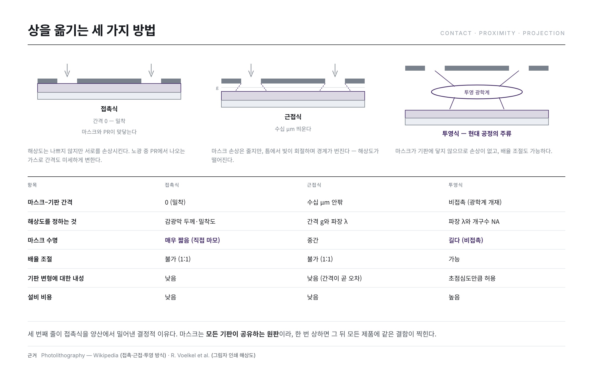
There are broadly three ways to transfer the mask pattern into the photoresist (Photolithography).
- Contact — the mask is pressed directly against the substrate and light is shone through. The setup is simple and the resolution is not bad, but mask and PR touch each other and damage both. On top of that, gases outgassing from the PR during exposure make the spacing shift slightly.
- Proximity — lift the mask a little. Mask damage drops, but light diffracts across the gap and resolution suffers.
- Projection — lenses or mirrors project the mask image onto the substrate. Since the mask never touches the substrate there is no damage, and the magnification can be adjusted. This is the mainstream of modern processing.
The three methods differ sharply in what you gain and what you give up.
| Item | Contact | Proximity | Projection |
|---|---|---|---|
| Mask-to-substrate gap | 0 (in contact) | tens of μm | none (optics in between) |
| What sets resolution | resist thickness, contact quality | gap g and wavelength λ | wavelength λ and NA |
| Mask life | very short (direct wear) | medium | long (non-contact) |
| Magnification control | none (1:1) | none (1:1) | available |
| Tolerance to substrate distortion | low | low (gap error is the error) | as much as the depth of focus |
| Equipment cost | low | low | high |
The third row is what pushed contact printing out of volume production. A mask is the master plate every substrate shares, so once it is damaged, every product that passes afterwards carries the same defect.
The limit of proximity printing can be calculated
There is no need to explain in words alone why proximity printing blurs. Light passing the openings in the mask undergoes Fresnel diffraction, and the edges spread out while it travels the gap g. In shadow printing the smallest resolvable line width is approximately
R ≈ √(λ · g) — λ: wavelength, g: gap between mask and resist
The square root matters. Halving the gap improves resolution only by √2, about 1.41×. Computing directly for the i-line (365nm):
| Gap g | R = √(λg) | With margin (1.5R) |
|---|---|---|
| 5 μm | 1.35 μm | 2.03 μm |
| 10 μm | 1.91 μm | 2.87 μm |
| 25 μm | 3.02 μm | 4.53 μm |
| 50 μm | 4.27 μm | 6.41 μm |
| 100 μm | 6.04 μm | 9.06 μm |
| 200 μm | 8.54 μm | 12.82 μm |
The values were computed directly from the formula with λ = 365nm. The dilemma of large areas shows up right here: the bigger the substrate, the wider the gap has to be. Holding a metre-class sheet of glass and a metre-class mask parallel at a few μm is not realistic, and the slightest touch ruins the mask. The moment you set the gap at 100μm, resolution is pinned near 6μm. The reason shadow-printing methods survive only for coarse patterns is contained in that one square root (R. Voelkel et al., 2015).
Lens or mirror — the fork in the road for large areas
Even within projection, displays hit a fork in the road: lens or mirror?
The lens approach transfers the image precisely and can freely magnify or reduce. The problem is that you cannot build a big lens. As a lens grows, it deforms under its own weight and aberrations get severe. So the area that can be exposed in one shot is limited, and a large sheet of glass has to be exposed in several separate shots (the step approach). At that point the positioning accuracy of the stage becomes the quality itself — if the separately shot fields are misregistered, the seams show.
The mirror approach can be scaled up, so a wide area can be scanned in one pass. In exchange, magnification is hard to adjust (essentially 1:1), and producing uniform illumination over a wide area is extremely difficult. Hence a scanning scheme in which the mask and stage are swept together past a slit.
The root of this structure is the unit-magnification reflective system worked out in the early 1970s. Build it from two concentric spherical mirrors at exactly 1:1 and, because mirrors have no refractive index, chromatic aberration cannot exist in principle, while coma and astigmatism cancel by symmetry. What remains is a narrow annular zone of good imagery; slice part of that ring with a slit and sweep mask and substrate together, and the exposure is as wide as the slit and as long as the scan (A. Offner, Opt. Eng. 14(2), 1975; US 3,748,015). "If you cannot print wide, sweep long" was the first answer large-area optics found.
Modern large-area exposure tools inherit that idea, using catadioptric systems that mix mirrors and lenses, and lining several such projection modules side by side to cover the width (S. Kohno et al., 2006). Making brightness and magnification join smoothly at the boundaries of the stitched images is the central difficulty of this approach (Large area fine line patterning by scanning projection lithography, 1996).
The two approaches differ wholesale in design — light source, illumination optics, mask stage, alignment system, chamber. It is less a question of which is right than a choice made according to panel size and the line width required.
Why displays choose a "blurry lens"
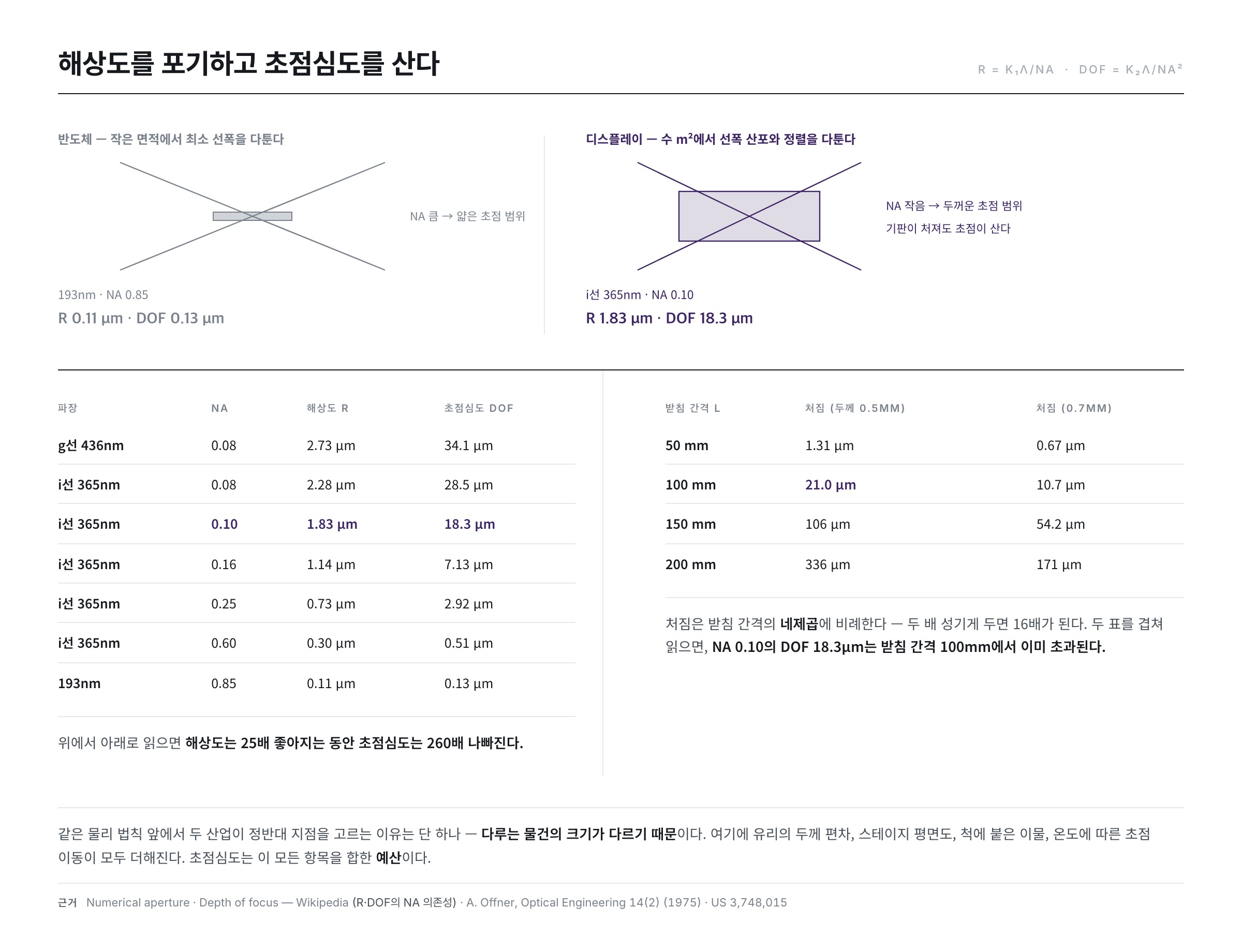
Here comes the most interesting part of this post. Optics has two formulas you cannot escape.
R = k₁ · λ / NA | DOF = k₂ · λ / NA²
- Resolution R — the shorter the wavelength and the larger the numerical aperture, the smaller the pattern you can draw.
- Depth of focus DOF — but as NA grows, the thickness range that stays in focus thins with the square.
This is the famous Rayleigh criterion and its price (Numerical aperture, Depth of focus). Put real numbers into the two formulas and it becomes obvious at a glance why the two industries split in opposite directions. The table below fixes the process constants at k₁ = k₂ = 0.5 and varies only wavelength and NA.
| Wavelength | NA | Resolution R | Depth of focus |
|---|---|---|---|
| g-line 436nm | 0.08 | 2.73 μm | 34.1 μm |
| i-line 365nm | 0.08 | 2.28 μm | 28.5 μm |
| i-line 365nm | 0.10 | 1.83 μm | 18.3 μm |
| i-line 365nm | 0.16 | 1.14 μm | 7.13 μm |
| i-line 365nm | 0.25 | 0.73 μm | 2.92 μm |
| i-line 365nm | 0.60 | 0.30 μm | 0.51 μm |
| 193nm | 0.85 | 0.11 μm | 0.13 μm |
Read the table top to bottom and resolution improves 25-fold while depth of focus degrades 260-fold. Compare the last two rows in particular. The 18.3μm depth of focus of the i-line at NA 0.10 is about 137 times deeper than the 0.13μm of 193nm at NA 0.85. Semiconductors aim at nanometre line widths, so they push NA to the extreme and pay for it by controlling wafer flatness at the nanometre level.
Displays choose the opposite. Since the required line width is on the micrometre scale, there is no reason to raise NA. Designing NA low instead buys a generous depth of focus. A sheet of glass a metre or more across sags under its own weight and distorts with heat no matter how well it is supported, and a deep depth of focus absorbs that distortion. On top of that, several wavelengths are used together to secure exposure dose.
In short, "give up resolution and buy depth of focus" is the strategy of large-area exposure. Facing the same laws of physics, the two industries pick opposite points for exactly one reason — the things they handle are different sizes.
The focus budget — what eats the depth of focus
Why a generous depth of focus is a necessity rather than a luxury becomes clear once you calculate how much the substrate actually bends. Suppose the glass rests on supports at a regular pitch, and treat each span between supports as a simply supported beam under a uniformly distributed load. The maximum deflection is
w = 5qL⁴ / (384EI) (q = ρgt, I = t³/12) → w = 0.15625 · ρgL⁴ / (E t²)
Insert a glass density of 2,500kg/m³, a Young's modulus of 73GPa and a thickness of 0.5mm, and vary only the support pitch L:
| Support pitch L | Deflection (0.5mm thick) | Deflection (0.7mm thick) |
|---|---|---|
| 50 mm | 1.31 μm | 0.67 μm |
| 100 mm | 21.0 μm | 10.7 μm |
| 150 mm | 106 μm | 54.2 μm |
| 200 mm | 336 μm | 171 μm |
Deflection scales with the fourth power of the pitch, so doubling the spacing multiplies the sag by sixteen. Overlay this table on the depth-of-focus table above. The 18.3μm available to i-line at NA 0.10 is already exceeded at a support pitch of 100mm. Had the tool been designed at NA 0.60 (0.51μm of depth of focus), sag alone would consume more than twice the entire focus budget even at a 50mm pitch.
To that add the thickness variation of the glass itself, the flatness of the stage, fine particles on the chuck, and focus drift of the optics with temperature. Depth of focus is the budget covering all of those items at once, and in large-area work that budget is always tight. So the tool measures substrate height in real time while scanning and drives the stage up and down to follow it; a generous depth of focus is the safety margin covering whatever that correction cannot keep up with.
Alignment — laying one layer over another
Exposure is not only about shining light. Before it comes alignment. A backplane is built by stacking layers, and the patterns of each layer must overlap accurately to become a circuit. If source and drain are offset over the gate, you have a reject rather than a transistor.
So the substrate carries reference marks called alignment keys, and the tool reads them through a microscope to compute position. The bow and warpage from the heat treatments of post 5 surface as a problem here — if the substrate deforms, the keys move and alignment goes off. Which is why the tool does more than match position: it measures and corrects the stretch, rotation and orthogonality of the whole substrate.
The items actually measured and corrected are usually six — X and Y translation, rotation, orthogonality, and X and Y magnification (scale). The first three are questions of how the substrate was placed; the last three mean the substrate has actually deformed. So the tool changes the projection magnification to several decimal places and deliberately distorts the image to match the deformation of the substrate.
Why magnification correction is needed follows from thermal expansion alone. Borosilicate-class glass has a linear expansion coefficient around 3.3ppm/K (Borosilicate glass). On a substrate 2.5m long, a change of only 1℃ changes the overall length by 8.25μm. Even 0.1℃ gives 0.83μm. In a process demanding micrometre alignment, that is why temperature control of the exposure room is alignment accuracy. The quality of the preceding steps and the stability of the air handling show up as exposure accuracy several stages later.
The mask — making two heights in one shot
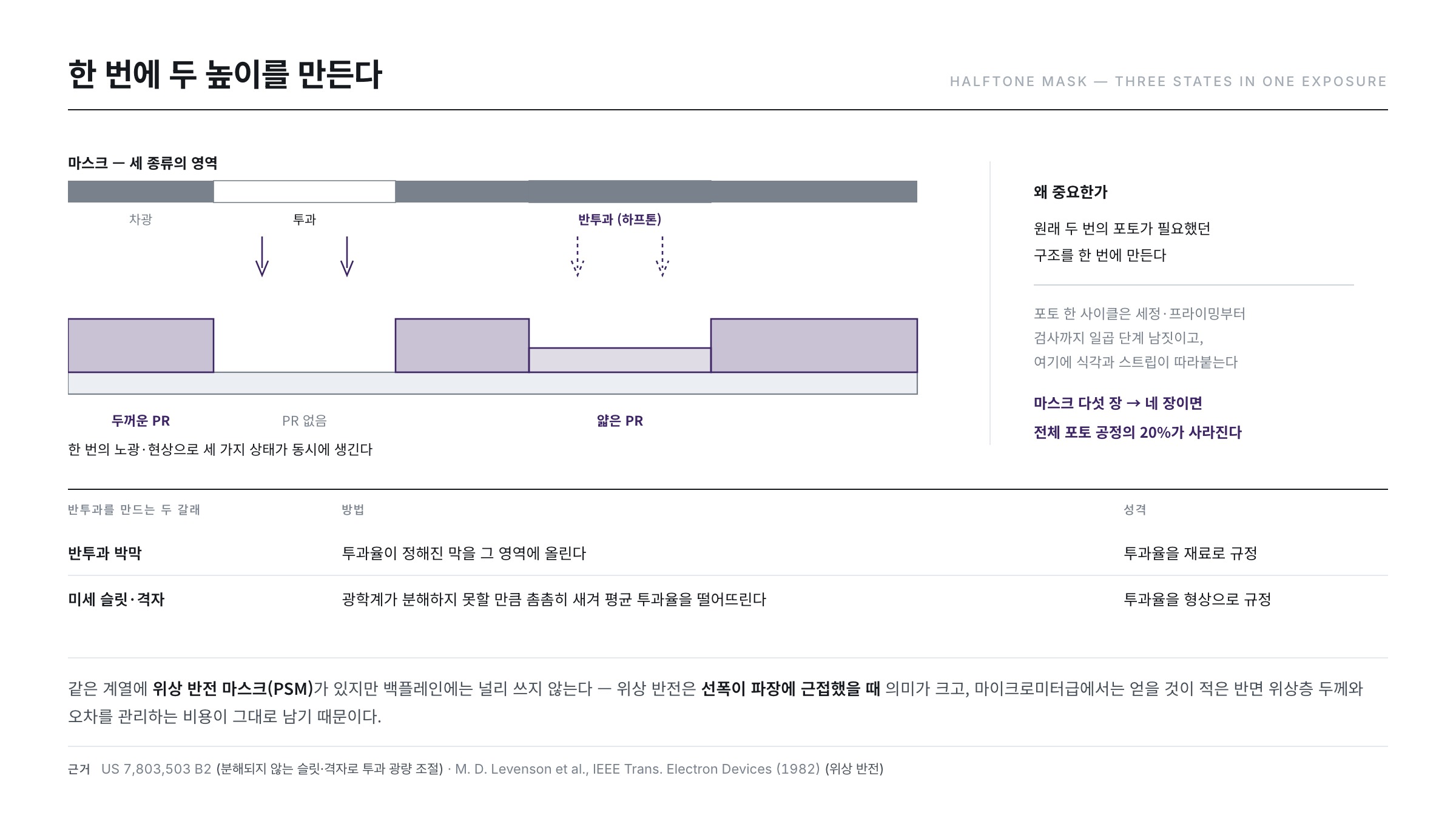
The simplest mask is a binary mask: places that pass light and places that block it, nothing else. When the wiring width is comfortably larger than the exposure wavelength, that is enough.
But add a semi-transmissive (halftone) region and something interesting becomes possible. If only part of the light gets through, the PR dissolves only partially and a thin layer remains. A single exposure and development can therefore produce three states at once — thick PR, thin PR, and no PR.
There are two ways to build the semi-transmissive region. One is to put a thin film of defined transmittance over that area; the other is to engrave slits or a grating too fine for the exposure optics to resolve, lowering the average transmittance. The latter is called a slit or gray-tone mask, and the patent literature defines it as having "a pattern arranged in slits or lattice which is not resolved at an optical lithography so as to control the transmitted amount of light in the portion where the pattern is disposed" (US 7,803,503 B2). Not being resolved is the crucial condition — if the slits image, ripples appear on the resist surface and the remaining thickness becomes uneven.
Why does this matter? Because a structure that used to need two photo cycles can be made in one. A partition wall defining the emitting area and a spacer above it, for example — two structures of different height — can be completed with a single mask. Removing one mask and one process cycle is a direct cost reduction in large-area volume production.
Estimate the saving and the scale becomes visible. One photo cycle runs about seven steps, from clean and priming through to inspection, with etch and strip following behind. Cutting an array that took five masks down to four erases 20% of the entire photo process.
Phase-shift masks — making phase a design variable
A related technology is the phase-shift mask (PSM). If the light through two adjacent apertures is made 180° out of phase, the amplitude at the boundary between them cancels exactly to zero. On a binary mask the light from the two apertures overlaps and the boundary actually brightens; flipping the phase forces a dark line to exist there (Phase-shift mask).
The idea was proposed in 1982, and it was confirmed experimentally that resolution and depth of focus improve together in the same optical system (M. D. Levenson, N. S. Viswanathan, R. A. Simpson, IEEE Trans. Electron Devices 29(12), 1828 (1982)). Two years later imaging simulations and actual resist exposures verified the effect down to submicrometre patterns (The phase-shifting mask II, IEEE Trans. Electron Devices 31(6), 753 (1984)). In terms of the formula above it is a technique for lowering k₁ while leaving λ and NA alone — remarkably economical, since resolution is gained without touching the optics.
So why does the display backplane not use it widely? Phase shifting only pays when the line width approaches the wavelength. At micrometre line widths there is little to gain, while the cost of forming the phase layer to an exact thickness and controlling phase error remains.
The light source — three peaks of the mercury lamp
For the light source, the ultra-high-pressure mercury lamp has been in use for a long time. Mercury lamps emit strongly at particular wavelengths, and those peaks have names — g-line 436nm, h-line 405nm, i-line 365nm (Mercury-vapor lamp). Converted to the energy of a single photon they are 2.84eV, 3.06eV and 3.40eV respectively. The shorter the wavelength the stronger the photon — but at equal power, the number of photons falls.
That number drives a practical choice. A resist has to decompose a fixed number of photoactive molecules, so what it needs is closer to a count of photons than to energy. Large-area exposure therefore tends to use several lines together rather than picking one, securing dose and raising scan speed. The cost is that each wavelength focuses at a different position (chromatic aberration), which makes the optics harder — and is one more reason reflective systems become attractive.
Lamps also have a life. As burning hours accumulate the arc tube clouds and the electrodes erode, so irradiance slowly falls; since dose is irradiance × time, missing that drift means under-exposure and line widths that quietly grow.
Another handle on resolution is the shape of the illumination. Making the source an annulus rather than a disc, so that more light arrives at oblique angles, has been shown experimentally to improve both image contrast for fine patterns and depth of focus at the same NA (W. N. Partlo et al., Proc. SPIE 1927, 137 (1993)). Mask, illumination and optics are not independent parts but one set that makes a single image.
Three common misconceptions
- "A display exposure tool is a cheap version of a semiconductor one." They are separate machines with different goals. Semiconductors fight for minimum line width over a small area; displays fight for line-width distribution and overlay over several square metres. The difficulty lies in area and stability, not resolution.
- "Higher NA is always better." The table answers this. Raising NA shrinks depth of focus with the square, and in large-area work substrate sag eats that loss immediately. You buy resolution you do not need while selling the depth of focus you do.
- "A mask is not a consumable." It has to be inspected and cleaned on a schedule, and cleaning itself wears it slightly. A mask is a master plate with a lifetime.
What the floor watches — three control points
- Dose and focus — source intensity falls slowly with lamp life. Without periodic irradiance measurement and correction, line width drifts quietly.
- Overlay accuracy — how precisely layer sits on layer. Substrate distortion from earlier steps, stage positioning accuracy and thermal stability all converge here.
- Mask condition — a single particle on the mask produces a defect in the same place on every panel. So masks are covered with a pellicle and inspected and cleaned periodically (Photomask).
The pattern has been drawn in PR. From the next post (post 14) we enter the etch chapter, where the film is actually removed according to that pattern. We start with the shared concepts and parameters.
References
- M. D. Levenson, N. S. Viswanathan, R. A. Simpson, "Improving resolution in photolithography with a phase-shifting mask," IEEE Trans. Electron Devices 29(12), 1828 (1982) : the original proposal of the phase-shift mask, showing improvement in both resolution and depth of focus
- M. D. Levenson et al., "The phase-shifting mask II: Imaging simulations and submicrometer resist exposures," IEEE Trans. Electron Devices 31(6), 753 (1984) : verification of the phase-shift effect by imaging simulation and actual resist exposure
- A. Offner, "New Concepts in Projection Mask Aligners," Optical Engineering 14(2) (1975) : the 1:1 reflective projection system built from concentric spherical mirrors — the archetype of large-area scanning exposure
- US 3,748,015 — Unit power imaging catoptric anastigmat : the same reflective projection system captured as an apparatus patent
- S. Kohno et al., "Catadioptric Projection Optical System for Flat Panel Exposure Tool," International Optical Design (2006) : a mixed reflective-refractive projection system for large panel exposure
- "Large area fine line patterning by scanning projection lithography," Microelectronics Reliability 36(4), 547 (1996) : forming fine line widths over large areas by scanning projection
- R. Voelkel et al., "Micro-optics and lithography simulation are key enabling technologies for shadow printing lithography," Adv. Opt. Technol. 4(1), 63 (2015) : basis for gap and diffraction governing resolution in proximity and shadow printing
- W. N. Partlo et al., "Depth of focus and resolution enhancement of i-line and deep-UV lithography using annular illumination," Proc. SPIE 1927, 137 (1993) : measured improvement of resolution and depth of focus with annular illumination
- US 7,803,503 B2 — Halftone mask and method for making pattern substrate using the halftone mask : gray-tone masks that control transmitted dose with unresolved slits and lattices
- Photolithography — Wikipedia : contact, proximity and projection exposure and the process flow
- Numerical aperture — Wikipedia · Depth of focus — Wikipedia · Phase-shift mask — Wikipedia : the NA dependence of resolution and depth of focus, and the phase-shift concept
- Mercury-vapor lamp — Wikipedia · Photomask — Wikipedia · Borosilicate glass — Wikipedia : the g, h and i line wavelengths, masks and pellicles, and the 3.3ppm/K expansion coefficient of glass