Every film we have stacked so far covers the entire substrate. As it stands, that is not a circuit — it is just a plate. Now the circuit pattern has to be drawn into those films. The process that does it is photo (photolithography), and the principle is astonishingly simple — it is exactly the same as photography.
Like taking a photograph
Picture a film camera. Shine light onto a light-sensitive material (the film) and the chemistry of the exposed areas differs from the unexposed ones. Dip it in developer and that difference emerges as a visible image.
The photo process uses that principle as is. Coat the substrate with photoresist (PR), shine ultraviolet light through a mask carrying the circuit pattern, rinse with developer — and a PR pattern in the shape of the circuit is left on the substrate. That PR then acts as a cover in the next process (etching). What is covered survives; what is exposed gets etched away.
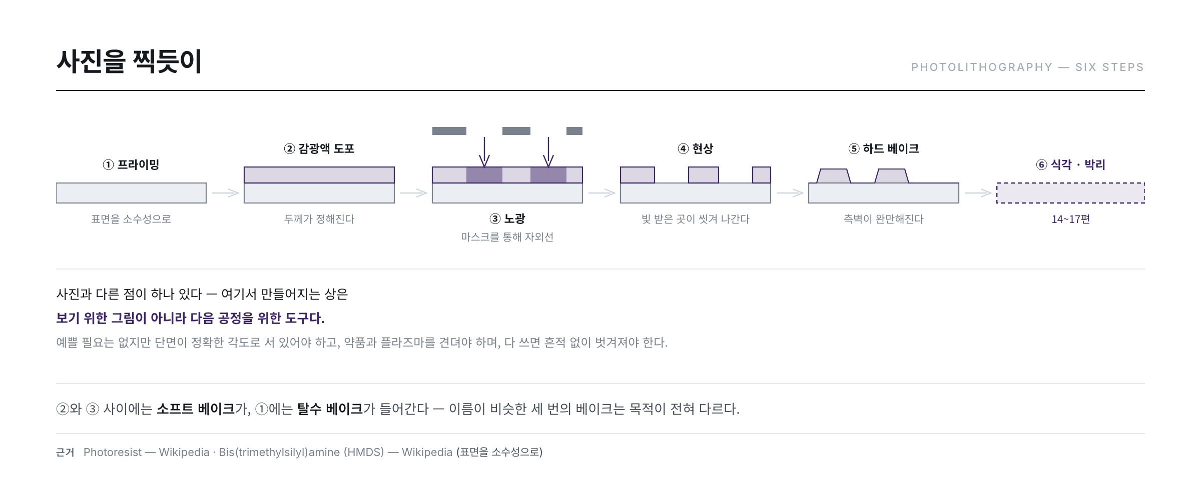
There is one difference from photography. The image the photo process makes is not a picture to look at but a tool for the next step. It does not have to be beautiful, but its cross-section has to stand at a precise angle, it has to survive chemicals and plasma, and once its job is done it has to strip away without a trace. Those three demands determine the entire design of the material we call photoresist.
Photoresist as a material
PR is made of three main parts.
- Resin — the skeleton that forms the film. Novolak-based resins are the classic choice.
- Photoactive compound (PAC) — the component that actually responds to light. Its concentration governs sensitivity.
- Solvent — the carrier that makes coating possible. After coating it only gets in the way, so it has to be driven out (exactly the same structure as the PI story in posts 2 and 3).
The properties you weigh when choosing a PR are many — sensitivity (how responsive to light), resolving power (how small a pattern it can form), contrast (the solubility gap between exposed and unexposed regions), heat resistance (can it survive plasma and ion implantation), adhesion (does it stick to the underlying film), chemical resistance (can it withstand the etchant), profile shape, and even shelf life. Improving one often degrades another, so different layers use different PRs.
Why light makes it dissolve — the chemistry of the PAC
"Expose it and it dissolves" is a result, not a reason. In the mainstream DNQ-novolak system, what actually happens is a two-stage change in polarity (Diazonaphthoquinone).
Novolak resin is an acidic polymer built on a phenolic backbone, so on its own it dissolves readily in alkaline aqueous solution. Add just a few percent of the photoactive compound DNQ, however, and dissolution almost stops. The DNQ molecules wedge themselves between the resin chains, blocking the path by which alkaline ions approach, and hydrogen-bond to the phenolic groups so the chains hold one another in place. This role is called a dissolution inhibitor.
When ultraviolet light arrives, DNQ loses a nitrogen molecule, its skeleton rearranges, and after reacting with water it becomes an indenecarboxylic acid. The molecule that was an inhibitor turns into an acid. Inside the alkaline developer that acid ionizes immediately, pulls in water, opens the blocked channels, and the dissolution rate of the exposed region climbs steeply. In other words the same single molecule acts as the brake before exposure and the accelerator after it. For g-line and i-line DNQ-novolak resists, the measured dissolution-rate gap between unexposed and exposed film is reported to span more than two orders of magnitude (see the 1989 JVST B characterization in the references).
Positive and negative
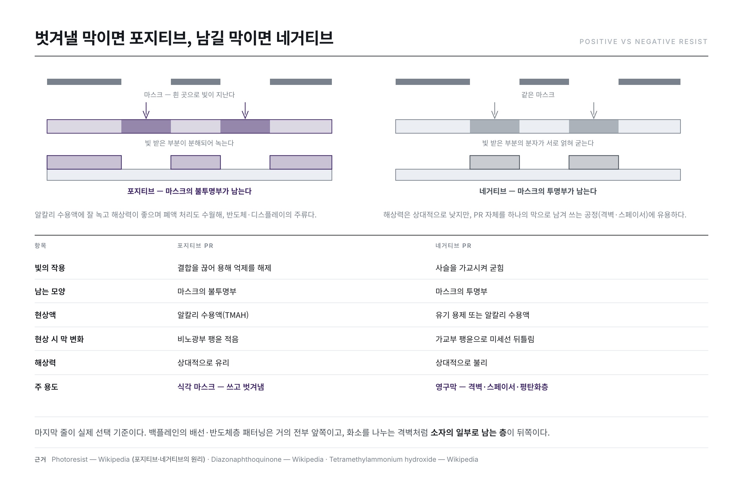
PR comes in two kinds, depending on which way it reacts to light (Photoresist).
- Positive tone PR (photo-decomposing) — the exposed areas break down and dissolve in the developer. The clear parts of the mask are left as openings in exactly that shape, hence "positive." It dissolves readily in alkaline aqueous solution, has good resolving power, and its waste is relatively easy to treat, which is why it is the mainstream choice in semiconductors and displays.
- Negative tone PR (cross-linking) — the molecules in the exposed areas tangle together (cross-link) and harden. What remains is the inverse of the mask, hence "negative." Its resolving power is comparatively lower, but it is useful for processes that leave the PR itself in place as a film (banks, spacers and the like).
| Item | Positive tone | Negative tone |
|---|---|---|
| Action of light | Breaks bonds, lifting dissolution inhibition | Cross-links chains, hardening the film |
| What remains | The opaque part of the mask | The clear part of the mask |
| Developer | Alkaline aqueous solution (TMAH) | Organic solvent or alkaline aqueous solution |
| Film change during development | Little swelling in unexposed areas | Cross-linked regions swell, distorting fine lines |
| Resolving power | Relatively favourable | Relatively unfavourable |
| Main use | Etch mask — used, then stripped | Permanent film — banks, spacers, planarization |
The last row of that table is the real selection rule. If the film is going to be stripped, positive; if it is going to stay, negative is the default. Patterning the wiring and semiconductor layers of a backplane falls almost entirely in the first category, while layers that remain as part of the device — the banks that separate pixels, for example — fall in the second.
Spin speed sets the thickness — the physics of coating
PR thickness is not a number you set by eye. How a viscous liquid film on a spinning disk thins out was worked out hydrodynamically as early as 1958. When centrifugal force and viscosity balance as the film spreads, the thickness after a time t converges to the following form.
h = √( 3μ / (4ρω²t) ) — μ: viscosity, ρ: density, ω: angular velocity, t: time
The key point to read out of it is that thickness varies inversely with the square root of the spin speed. A model published in 1978 added solvent evaporation and confirmed that real resist films keep the same exponent. Taking a condition that gives 1.50 μm at 1,000 rpm and changing only the spin speed, the thickness moves like this.
| Spin speed | Calculated thickness | Relative to 1,000 rpm |
|---|---|---|
| 500 rpm | 2.12 μm | 1.41× |
| 1,000 rpm | 1.50 μm | reference |
| 1,500 rpm | 1.22 μm | 0.82× |
| 2,000 rpm | 1.06 μm | 0.71× |
| 3,000 rpm | 0.87 μm | 0.58× |
| 4,000 rpm | 0.75 μm | 0.50× |
These values come straight from the spin-speed term of the equation above. Halving the thickness means quadrupling the spin speed — and, read the other way, a 5% error in spin speed produces only a 2.5% error in thickness. That insensitivity is why spin coating has survived so long.
Display substrates, however, cannot use it. Spin a 2.2 m × 2.5 m sheet of glass at 1,000 rpm and the rim of the diagonal (1.67 m from the centre) travels at 174 m/s, under a centrifugal acceleration of about 18,300 m/s², some 1,860 times gravity. Even at 500 rpm it is still 465 times. The glass would not survive, and even if it did, conditions would differ with distance from the axis so the thickness could never be uniform. Large-area processes therefore use slit coating instead of spinning — a long nozzle traverses the substrate once and lays the liquid down.
Material efficiency is decisive too. Leaving a 1.5 μm film on a 300 mm diameter disk requires a volume of only 0.11 mL (π × 0.15² × 1.5 μm); everything else is flung off by centrifugal force. Slit coating puts down only what is needed, so covering a 5.5 m² substrate — 78 times the area — to the same thickness takes just over 8.25 mL.
Putting numbers on a resist — Dill parameters and contrast
To handle a resist quantitatively, phrases like "it responds well" are not enough. The method proposed in 1975, still the standard today, describes a resist with three numbers.
| Symbol | Name | Physical meaning | When it is large |
|---|---|---|---|
| A | Bleachable absorption | The share absorbed by the PAC — it disappears as exposure proceeds | Bigger transmittance change before and after exposure |
| B | Non-bleachable absorption | Absorption by resin, dyes and so on that never goes away | Light cannot reach the bottom of the film |
| C | Exposure rate constant | Fraction of PAC decomposed per unit dose | Reacts with little light (high sensitivity) |
The remaining fraction of PAC, M, falls with dose E as M = exp(−C·E). Being exponential, there is no dose at which the PAC reaches exactly zero, so the process is managed against targets such as "the dose that decomposes 99%." A film with large A bleaches itself transparent as exposure proceeds, letting light reach the bottom; a film with large B stays dark at the base no matter how long you expose, and the cross-section tilts. Half of the sidewall angle is already decided by the absorption design of the resist.
The single number used most often in practice is contrast, γ. It is defined from the dose D0 at which film loss begins and the dose D100 at which the film is completely cleared.
γ = 1 / log₁₀(D100 / D0)
If the two doses differ by a factor of 2, γ = 1/log₁₀2 = 3.32; a factor of 3 gives 2.10; narrowing the gap to 1.5 gives 5.68. A larger γ means "a little more light and it clears completely," and that translates into a near-vertical cross-section and a tight line-width distribution. This nonlinearity is exactly what turns the blurred edge of a mask image into a crisp pattern.
Chemical amplification — using one photon many times
DNQ-novolak has a limit built into its principle. One photon converts one PAC molecule, so the reaction efficiency (quantum yield) can never exceed one. As the wavelength shortens the number of photons available from the source falls while the number of molecules to convert stays the same, and exposure times become impossible.
The solution proposed in 1983 is chemical amplification. Light does not change the resist directly; it merely generates one molecule of acid, and that acid then acts as a catalyst, stripping protecting groups off the resin one after another. The acid is not consumed by the reaction, so a single photon can trigger tens to hundreds of chemical events. The concept, which raised sensitivity at the level of principle, was consolidated into a patent granted in 1985 (US 4,491,628) and became the standard for every lithography generation from deep ultraviolet onward.
So why do displays still mostly use DNQ-novolak? Chemically amplified resists work by acid diffusion, which makes them extremely sensitive to post-exposure bake temperature and time; and if trace airborne base such as ammonia neutralizes the acid at the surface, the top of the pattern is blunted. For a backplane where line widths of a few micrometres are entirely sufficient, there is no reason to pay that management cost. Using a material exactly as sophisticated as the required resolution demands is what design means.
Three bakes, three purposes
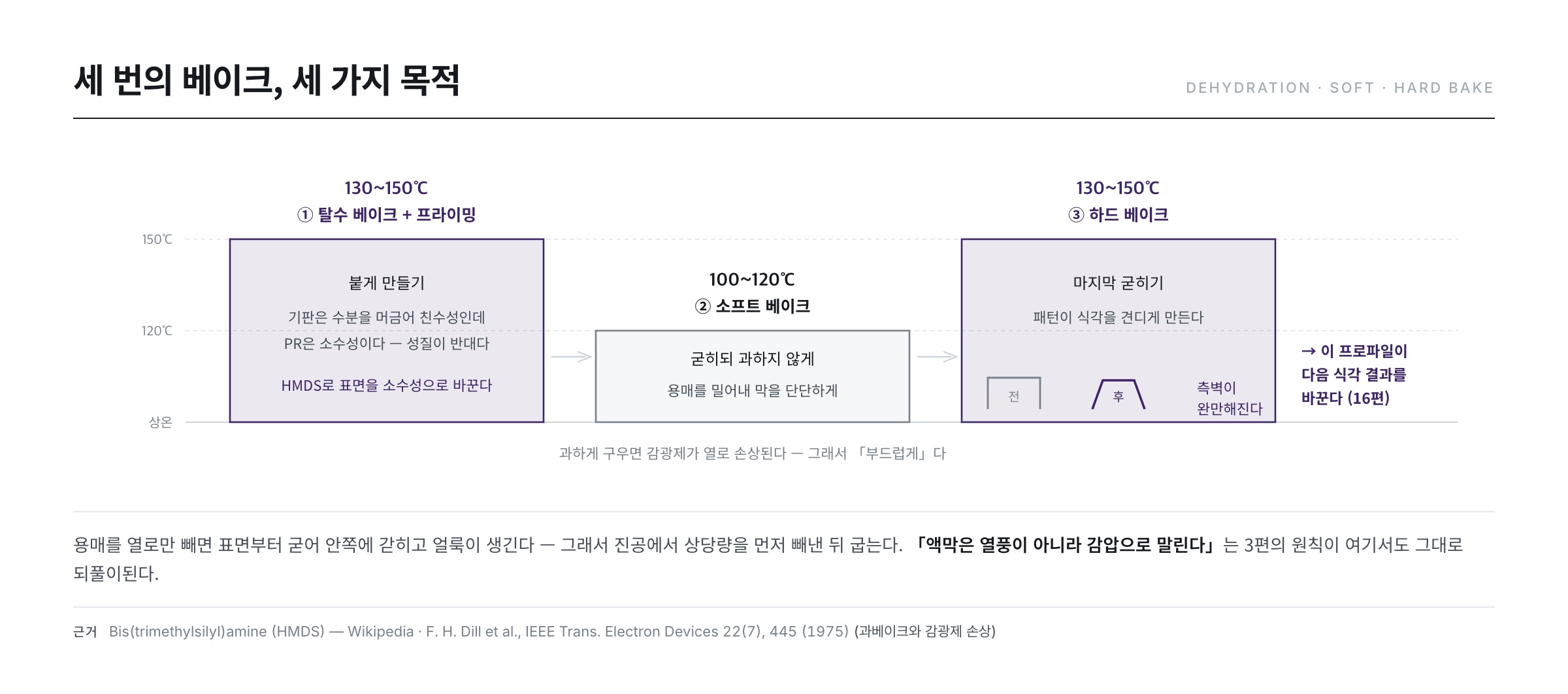
The photo process includes three separate baking steps. The names are similar enough to confuse, but their purposes are completely different.
① Dehydration bake and priming — making it stick
PR is a hydrophobic material; it does not like water. The substrate surface, however, has usually picked up moisture from the air and is hydrophilic. Opposite natures, so they do not adhere well. The fix is to first bake the substrate at around 130–150℃ to drive the moisture off (the dehydration bake).
When that alone is not enough, a chemical called HMDS is applied as a vapor. HMDS reacts with the hydrophilic groups on the substrate surface and turns the surface hydrophobic — matching its nature to the PR's. Wikipedia describes it as an "adhesion promoter that renders the surface hydrophobic and thereby promotes photoresist adhesion" (HMDS). The smaller the patterns, or the more isolated features a layer has, the more this preparation matters.
② Soft bake — firm up, but not too much
Right after coating, solvent still remains inside the PR. In that state it is soft and collapses easily under the developer and etch chemicals. So it is baked at a relatively low 100–120℃ to push out the solvent and harden the film.
This calls for a delicate balance. Overbake and the exposure and development characteristics degrade sharply — because the photoactive compound is damaged by the heat. Hence the name: bake it "softly." In the language of the Dill parameters above, overbaking destroys PAC that should have reacted later, which shaves A down and pushes B up; the result shows up as reduced contrast and a tilted cross-section.
Incidentally, the reduced-pressure drying from post 3 reappears here. If you drive the solvent out with heat alone, the surface hardens first, trapping solvent underneath and creating mottling — so a good deal of it is pulled out under vacuum first, and only then baked. The principle "you dry a liquid film with reduced pressure, not hot air" keeps recurring across processes.
③ Hard bake — the final hardening
Once development is done and the pattern is complete, it is baked once more at 130–150℃. The temperature is higher than the soft bake, hence "hard." The purpose is to make the pattern finally tough enough to survive etching.
But there is a hidden effect. At higher temperature the PR softens and flows slightly, so the sidewall angle of the pattern (its profile) becomes gentler. And that profile changes the outcome of the next etch — the wet etch profile control we will see in post 16 is directly coupled to these hard bake conditions. Photo and etch are not separate processes; they are one continuous design.
Wiping the edge clean — EBR
Large-area coating has a chronic problem: PR piles up thickly at the substrate edge. Surface tension makes the solvent evaporate first at the edge, and the PR crowds there. Some also ends up on the back side.
That thick rim becomes a particle source in later processes, interferes with the equipment that grips the substrate, and obstructs alignment key recognition. So immediately after coating, thinner is sprayed and instantly sucked away to wipe the PR off the edge and the back side — this is EBR (Edge Bead Removal). It looks like a minor step, but skip it and you will scatter particles down the whole line.
Development — turning a difference into an image
Expose the substrate to developer and the solubility difference emerges as a real pattern. The developer for positive tone PR is an alkaline aqueous solution, and in semiconductor and display processes TMAH (tetramethylammonium hydroxide) is the standard, because it contains no metal ions and therefore carries little contamination risk.
The concentration is generally set near 2.38%. That number has hardened into a de facto industry standard, and Wikipedia records that "0.26 N (2.38 wt%) TMAH is the industry-standard concentration for photoresist developer" (Tetramethylammonium hydroxide). You can check for yourself that the two notations are the same value — TMAH has a molar mass of 91.15 g/mol, so 23.8 g dissolved in one litre of water gives 23.8 ÷ 91.15 = 0.261 mol/L, matching 0.26 N.
Development is not simple "dissolving" either. The dissolution-rate model formalized in 1987 treats the rate as an S-shaped curve in the remaining PAC fraction M: slow at first, then climbing steeply, then saturating. The steeper that curve, the larger the contrast γ we saw earlier. If a small increase in dose produced a large change in line width, it means the operating point sits on the steep section of that S-curve.
Developer management has one trap. TMAH absorbs carbon dioxide from the air, forms carbonates, and its pH shifts. A change in concentration changes the development rate, and that shows up immediately as a change in line width. So sealing, circulation and concentration monitoring are essential. There are also several ways to develop — spray from nozzles, dip in a bath, puddle where the liquid is laid on the surface by surface tension — each with different chemical consumption and uniformity.
Two common misconceptions
- "Thicker resist is safer." True if you look only at etch resistance, but a thick film struggles to get light to its base (non-bleachable absorption B accumulates), and the longer development it needs over-erodes the top. The result is a tilted cross-section and a widened line. Thickness is a number set at the minimum resistance actually required.
- "More dose makes it sharper." Contrast is a property fixed by the material and the development conditions, not by the dose. Increasing the dose only moves the operating point along the curve, and too much of it damages the unexposed regions as well, collapsing the line width instead.
What the fab watches — Three Control Points
- Critical dimension (CD) — was it drawn at the designed width? Exposure dose, development conditions and PR thickness all converge on this single number. It is managed against the value measured right after development.
- Adhesion and defects — has the PR come off (lifting), have fine lines broken? Priming and bake conditions feed straight into this.
- Developer condition — concentration, temperature, metal ions, particles. As the chemistry ages, line width drifts quietly.
The next post (post 13) goes into the heart of this process, the exposure tool — how the mask image is transferred to the substrate, why displays choose exactly the opposite lens design from semiconductors, and how a halftone mask creates two different heights in a single shot.
References
- F. H. Dill et al., "Characterization of positive photoresist," IEEE Trans. Electron Devices 22(7), 445 (1975) : the origin of the standard model describing a resist with the three parameters A, B and C
- C. A. Mack, "Development of Positive Photoresists," J. Electrochem. Soc. 134(1), 148 (1987) : the S-shaped dissolution rate model in remaining PAC fraction — the basis for the development curve described here
- A. G. Emslie, F. T. Bonner, L. G. Peck, "Flow of a Viscous Liquid on a Rotating Disk," J. Appl. Phys. 29(5), 858 (1958) : the hydrodynamic solution showing spin-coated thickness varies inversely with the square root of spin speed — the equation behind the thickness table
- D. Meyerhofer, "Characteristics of resist films produced by spinning," J. Appl. Phys. 49(7), 3993 (1978) : a resist coating model showing the same exponent holds once solvent evaporation is included
- "Characterization of diazonaphthoquinone–novolac resin-type positive photoresist for g-line and i-line," J. Vac. Sci. Technol. B 7(3), 565 (1989) : measured dissolution behaviour of DNQ-novolak resist before and after exposure
- H. Ito, C. G. Willson, "Chemical amplification in the design of dry developing resist materials," Polym. Eng. Sci. 23(18), 1012 (1983) : the proposal of chemical amplification, where one photon triggers many chemical events
- US 4,491,628 — Positive- and negative-working resist compositions with acid generating photoinitiator and polymer with acid labile groups pendant from polymer backbone : the patent that consolidated chemically amplified resists as a composition
- Photoresist — Wikipedia : how positive and negative tone photoresists work, and what they are made of
- Diazonaphthoquinone — Wikipedia : the route by which a dissolution inhibitor photo-converts into indenecarboxylic acid
- Tetramethylammonium hydroxide — Wikipedia : the basis for 2.38 wt% = 0.26 N TMAH being the industry-standard developer concentration
- Bis(trimethylsilyl)amine (HMDS) — Wikipedia : the adhesion promoter that turns the surface hydrophobic