Before we can take on the thin-film transistor, the switch that draws the picture on a screen, there is one thing to settle first. What a semiconductor is.
The name itself invites a misunderstanding. 半導體 — matter that conducts halfway. So it is easy to settle for "something midway between a conductor and an insulator, a material that conducts middlingly" and move on. But understand it that way and nothing that follows can be explained. If it were a material of middling resistance, then nichrome wire would have to be a semiconductor too.
This series starts from semiconductors as a material and walks to the transistor as a device. This first article is the starting point — what exactly separates a semiconductor from other matter, why silicon of all things, and why the very same silicon splits into three kinds.
The condition values appearing in the calculations here (concentrations, dimensions, voltages, and so on) are examples meant to show how the calculation works, and the materials and structures are likewise the forms described in the open literature — not any particular company's specifications or drawings. Everything is kept to a level anyone can verify in published papers, patents, and encyclopedias, and each article closes with its sources.
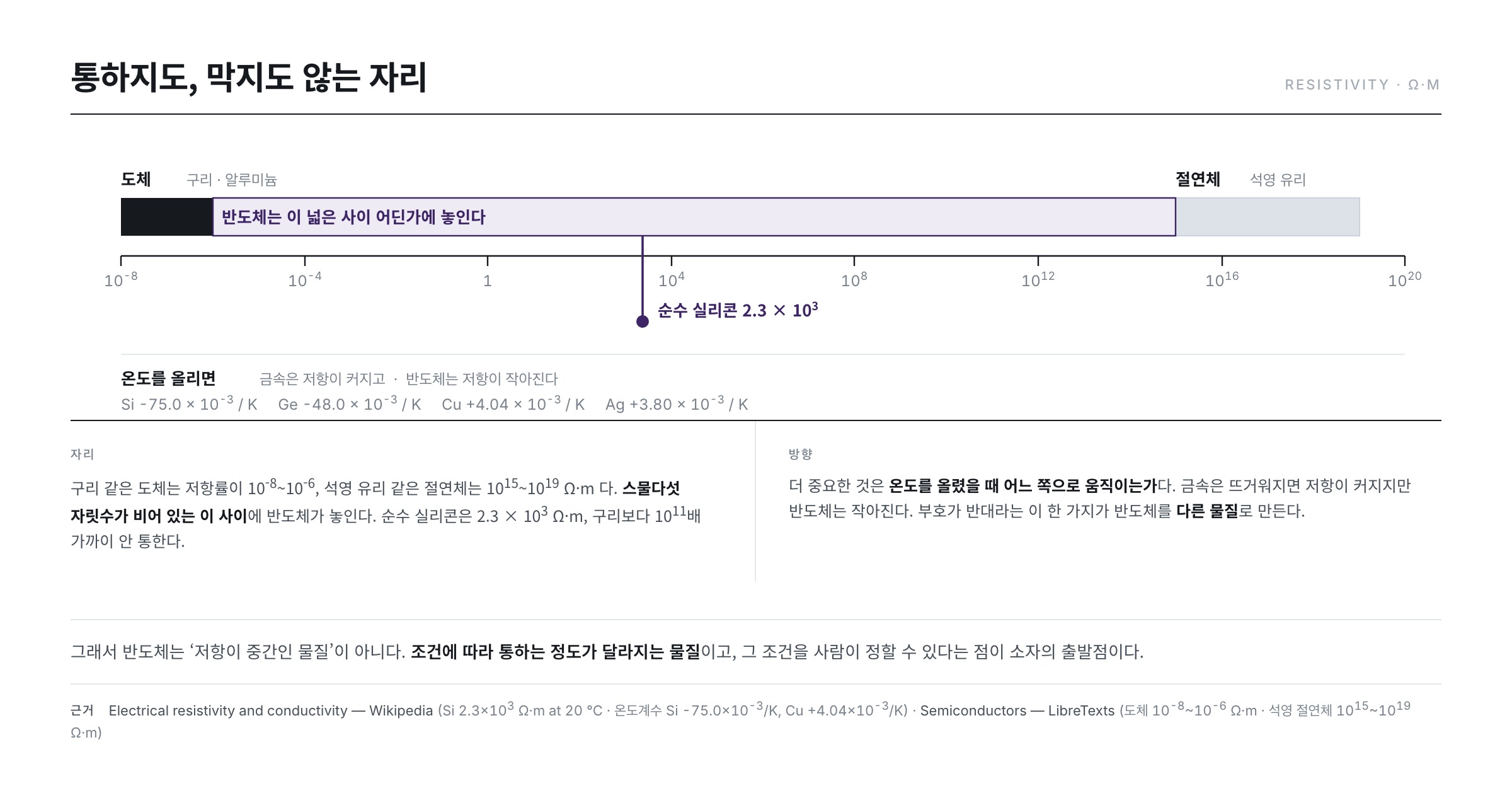
Not in the middle — the middle is empty
The value expressing how poorly a material conducts electricity is called resistivity, and its unit is Ω·m. The larger the value, the less it conducts. Resistivity is a property of the material itself, while the resistance we read off an instrument is that value multiplied by the shape of the object. The Wikipedia article "Electrical resistivity and conductivity" writes the relation between the two as R = ρ ℓ / A. Here ρ is resistivity, ℓ is length, and A is cross-sectional area. Longer means more resistance and thicker means less — an expression that makes sense the moment you picture a hose.
For a bar 1 cm long with a cross-section of 1 mm2, ℓ = 0.01 m and A = 10-6 m2.
- Copper (ρ = 1.68 × 10⁻⁸ Ω·m) → R = 1.68 × 10-8 × 0.01 ÷ 10-6 = 1.68 × 10⁻⁴ Ω, that is 0.17 mΩ
- Pure silicon (ρ = 2.3 × 10³ Ω·m) → R = 2.3 × 103 × 0.01 ÷ 10-6 = 2.3 × 10⁷ Ω, that is 23 MΩ
The same bar, and one comes out at 0.17 mΩ, the other at 23 MΩ — a ratio of 140 billion.
Take in the table of the "Electrical resistivity and conductivity" article more broadly and metals such as copper and silver are clustered around 10-8, while at the far opposite end sit insulators such as fused quartz at 1015~1019. They look like two clumps, but twenty-five orders of magnitude are missing wholesale in between. That is the difference between 1 and 10,000,000,000,000,000,000,000,000. The semiconductor sits in that empty stretch — in the table of the "Electrical resistivity and conductivity" article, pure silicon comes in at 2.3 × 10³ Ω·m at 20 °C, nearly 1011 times less conductive than copper.
Raise the temperature and it moves the other way
The "Electrical resistivity and conductivity" article also carries a temperature coefficient of resistivity for each material. It is the value expressing what percentage the resistivity shifts when the temperature is raised by 1 K.
- Copper +4.04 × 10⁻³ / K, silver +3.80 × 10⁻³ / K — get them hot and the resistance rises.
- Silicon -75.0 × 10⁻³ / K, germanium -48.0 × 10⁻³ / K — get them hot and the resistance falls.
The expression the "Electrical resistivity and conductivity" article carries is ρ(T) = ρ0 [ 1 + α (T − T0) ]. To the resistivity ρ0 at the reference temperature T0 you add the amount the temperature has moved, multiplied by the coefficient α. Let us substitute a rise of just 1 K.
For copper, 1 + 4.04 × 10-3 = 1.00404, so the resistivity grows by 0.4%; for silicon, 1 − 75.0 × 10-3 = 0.925, so it drops by 7.5%.
The signs are opposite and the magnitude differs by more than an order of magnitude. A metal's resistance merely creeps up as it warms, but raise silicon's temperature and it turns into a noticeably better conductor. That said, you must not take this expression at face value and push the temperature far. The "Electrical resistivity and conductivity" article states flatly that the relation is only an approximation, holding within a narrow range around the reference temperature. What to read here is the sign and the order of magnitude.
Why the signs are opposite
A metal already has electrons to spare. Raising the temperature adds none; what it does instead is make the atoms vibrate more widely about their positions. The "Electrical resistivity and conductivity" article explains this as the electron–phonon interaction and describes the lattice vibrations as scattering the electrons. The road is unchanged while the obstacles multiply, so the resistance rises.
A semiconductor has its problem at the opposite end. It is short of electrons to move in the first place. The "Electrical resistivity and conductivity" article describes how, in a semiconductor, thermal energy pushes electrons up into the conduction band so that they flow freely, and the holes left behind flow freely as well. Raising the temperature does add obstacles, but it adds travellers far faster. So the combined result comes out on the side of "resistance falls."
This is the line separating "middling" from "semiconducting." Nichrome wire has a large resistance, but raising its temperature does not change its character. A semiconductor's does change. The Wikipedia article "Semiconductor" likewise defines a semiconductor as a material whose conductivity lies between that of a conductor and an insulator and whose conductivity doping can alter. "Can be altered" is already built into the definition. How well it conducts changes with the conditions, and a person can set those conditions — this is where devices begin.
Why silicon of all things
Plenty of materials can be semiconductors. Germanium is one, gallium arsenide another. Yet silicon is used overwhelmingly more than the rest. The reason lies in a single atom.
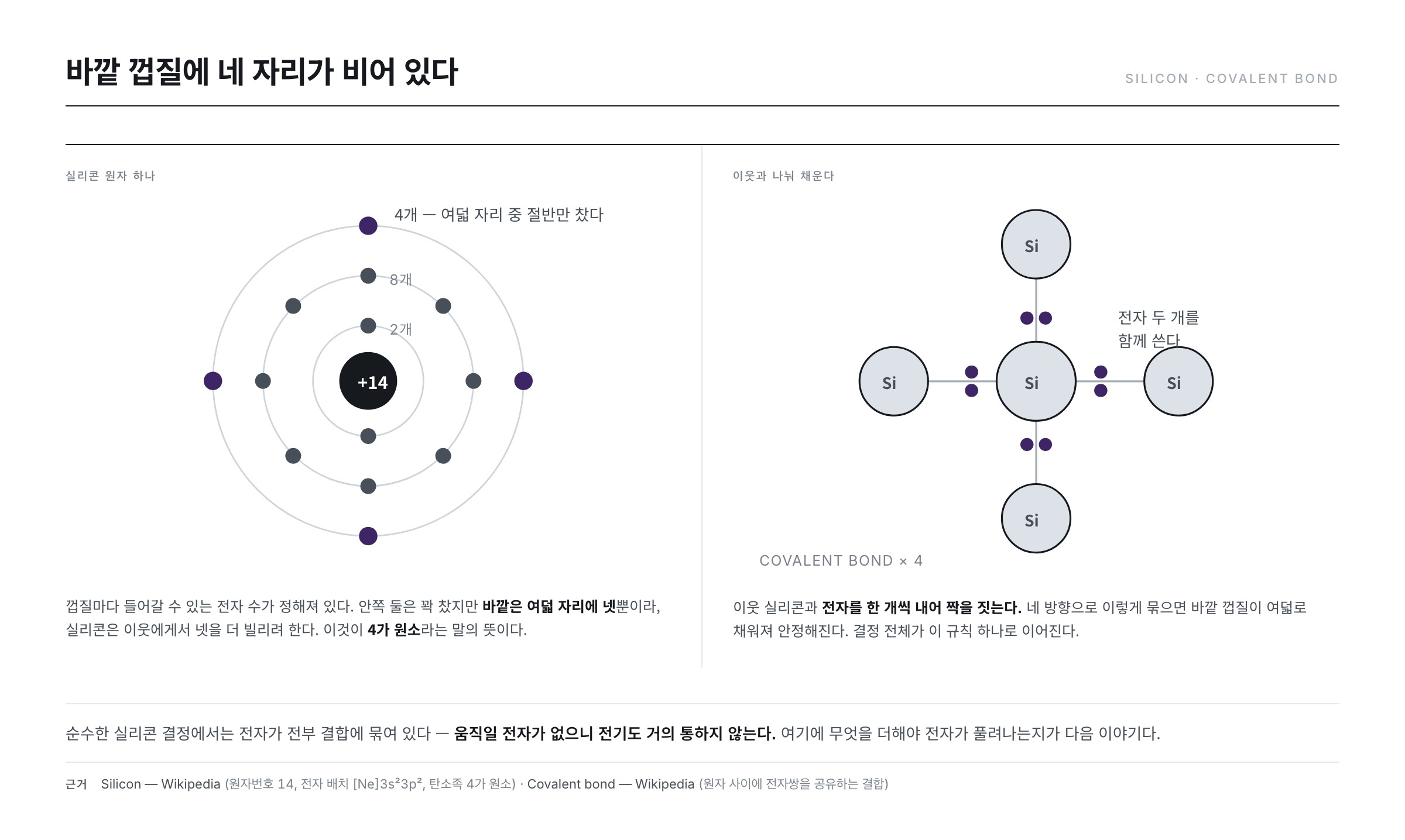
The Wikipedia article "Silicon" gives silicon's atomic number as 14 and its electron configuration as [Ne] 3s2 3p2. That is a structure in which the nucleus carries a charge of +14 and fourteen electrons surround it in shells.
Each shell has a fixed number of electrons it can hold. The inner two shells are full at 2 and 8, while the outermost shell has only four of its eight places occupied. These four outer electrons are called valence electrons; the "Silicon" article writes that the four occupy the 3s orbital and the 3p orbitals, and classifies silicon as a tetravalent element of group 14.
The outer shell is stable only when eight places are filled. A silicon atom four short pairs up with its neighbours, each side putting in one electron. This bond, in which two atoms share a pair of electrons, is the covalent bond. Silicon makes this bond in four directions, leading — in the "Silicon" article's phrasing — to a tetrahedral structure by way of sp3 hybridization.
Counting for ourselves how densely the atoms pack
When tetrahedral bonds continue without end, you get a crystal. The "Silicon" article gives that crystal structure as face-centred diamond cubic and the lattice constant as 543.0986 pm at 20 °C. A single unit cell of this structure holds 8 atoms. Converting the lattice constant to centimetres gives 5.431 × 10⁻⁸ cm, so
atomic density = 8 ÷ (5.431 × 10⁻⁸)3 = 8 ÷ (1.602 × 10⁻²²) = about 5.0 × 10²² atoms/cm3
The value the Wikipedia article "Doping (semiconductor)" gives for the atomic density of intrinsic crystalline silicon is about 5 × 10²² atoms/cm3. A calculation that started from the length of one lattice edge lands on the value in the literature. This number comes back in the next article.
Which is why pure silicon barely conducts
Here is the point where a first-time reader most often stumbles. A pure semiconductor conducts almost no electricity. When the whole crystal is knit together by covalent bonds without a gap, every electron is tied into a bond and holds its own post. The 2.3 × 10³ Ω·m seen earlier is that state.
It is not quite zero, though. The heat at room temperature breaks a few bonds and sets some electrons loose. How many that amounts to, and why the number climbs steeply as the temperature rises, is handled in the next article by way of energy bands.
The reason silicon was the one chosen lies here as well. The Wikipedia article "List of semiconductor materials" gives silicon's band gap as 1.12 eV. Think of the band gap as the threshold energy it takes to break a bond and set an electron loose. Line 1.12 eV up against the other materials the "List of semiconductor materials" article carries and you can see where it sits.
- Germanium 0.67 eV (indirect), silicon 1.12 eV (indirect), gallium arsenide 1.42 eV (direct)
- Diamond 5.47 eV (indirect) — nearly five times wider than silicon's.
Silicon's 1.12 eV is exquisitely placed for room temperature — wide enough that heat alone barely gets anything through, narrow enough that a touch changes things greatly. Germanium, at 0.67 eV, is narrower, so even at room temperature a good deal of current leaks through. In the resistivity table too, germanium comes in at 4.6 × 10⁻¹ Ω·m, 5,000 times more conductive than silicon — which means it cannot block when blocking is what you need. Diamond, at the other extreme, is at 5.47 eV, so room-temperature heat makes nothing happen at all.
There are more reasons than the band gap
The strength is not the band gap alone. Three properties set down in the "Silicon" article line up alongside it.
- It is abundant — the "Silicon" article writes that silicon makes up 27.2% of the Earth's crust by mass, second only to oxygen at 45.5%. The raw material is, in effect, sand.
- It melts high — at 1687 K (1414 °C). Most of the processes for making a device pass through high temperatures, and silicon does not lose its shape along the way.
- It grows its own good insulating film — the "Silicon" article writes that silicon forms a thin, continuous layer of silicon dioxide (SiO2) on its surface that protects what lies beneath from oxidation. Below 900 °C it does not react with air.
That last item matters especially. A device needs both a part that conducts and a part that blocks, and silicon gets the blocking material from its own surface.
The same silicon, and yet three kinds
One more thing is often left out of the silicon story. The same silicon behaves like a completely different material depending on how it solidified. This distinction becomes the backbone of the thin-film transistor story.
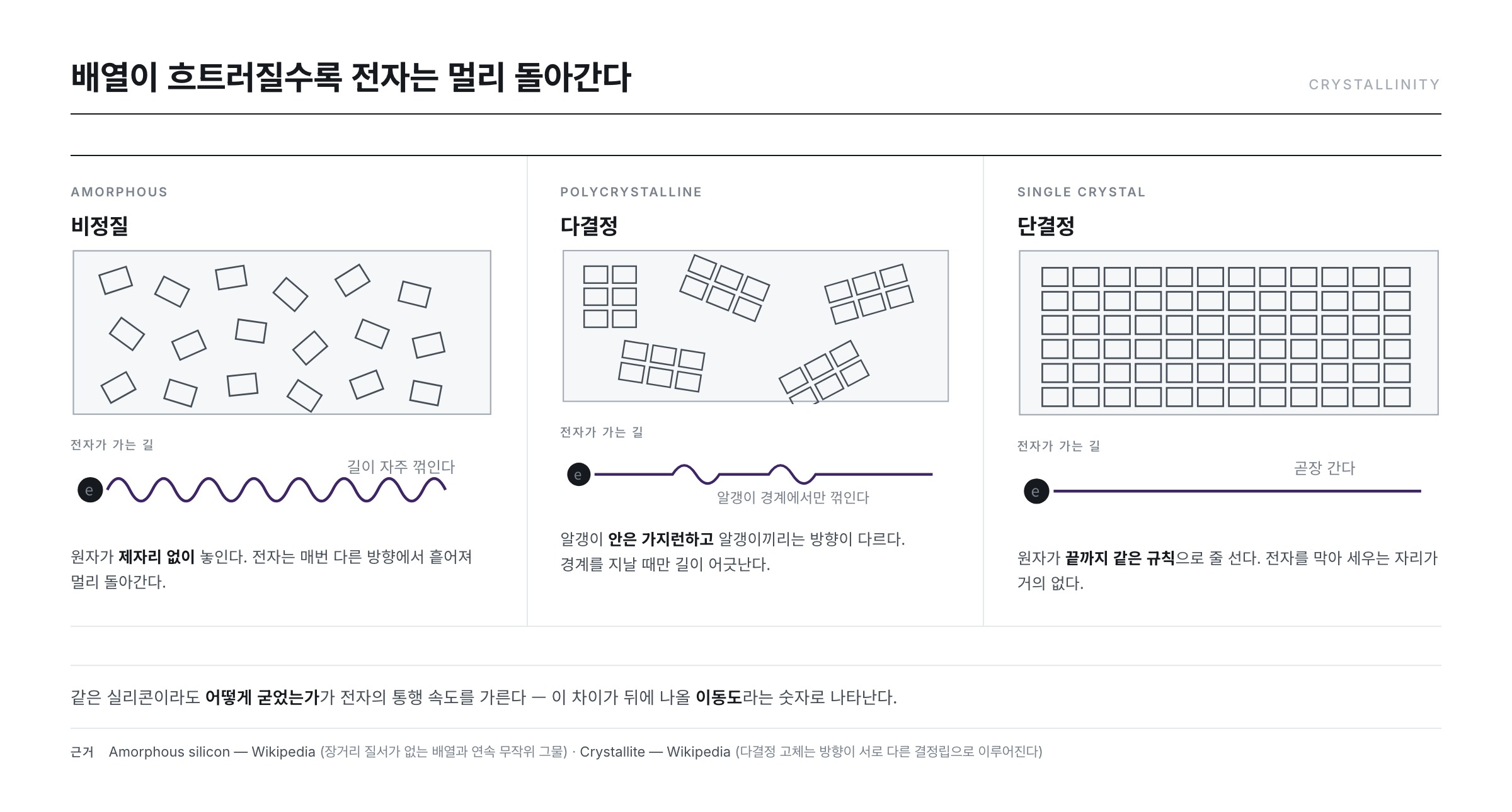
- Single crystal — the atoms line up by the same rule from one end to the other. The wafer that computer chips are carved out of is this.
- Polycrystalline — the Wikipedia article "Crystallite" describes a polycrystalline solid as an assembly of crystallites of varying size and orientation. Inside a grain things are orderly, but grain to grain they are misaligned.
- Amorphous — there is no rule. The Wikipedia article "Amorphous silicon" describes it as lacking long-range order, with the atoms forming a continuous random network.
What happens where the alignment breaks
For the polycrystalline case, the "Crystallite" article calls the interface where crystals of differing orientation meet the grain boundary, and describes that region as gathering atoms displaced from lattice sites, dislocations, and impurities that have migrated there. Inside a grain nothing differs from a single crystal, but between the grains lie these disorderly bands. The Wikipedia article "Polycrystalline silicon" writes that the resistivity and mobility of polycrystalline silicon depend strongly on grain size, and describes recombination as occurring more at the grain boundaries.
In amorphous material the defects are not confined to boundaries but are scattered throughout. The "Amorphous silicon" article describes how the disordered structure leaves bonds that found no partner, that is dangling bonds, and how these can cause anomalous electrical behaviour. The remedy is set down alongside it — hydrogen attaches to the dangling bonds and lowers the defect density by several orders of magnitude. This material is called hydrogenated amorphous silicon (a-Si:H).
The difference shows up as speed
This difference shows up in the speed of the electrons. That value is mobility, and its unit is cm2/(V·s). The Wikipedia article "Electron mobility" defines mobility as vd = μe E, that is, the ratio of the drift velocity vd that arises when an electric field E is applied to E itself.
The mobility table in the "Electron mobility" article gives the electron mobility of crystalline silicon as 1,400 and the hole mobility as 450. In the table of the "Electron mobility" article, polycrystalline silicon is 100 and amorphous silicon is about 1.
Since we have the defining expression, we can turn these numbers into speeds. Apply an electric field of 1 V/cm and an electron in crystalline silicon drifts at v = 1,400 × 1 = 1,400 cm/s, that is 14 m per second. Under the same field, an electron in amorphous silicon manages 1 cm/s.
1,400 against 1. The substance is the very same silicon, yet the difference runs to more than a thousandfold. The more the arrangement is disturbed, the more often an electron's path bends as it travels. The "Electron mobility" article divides the scattering that lowers mobility into phonon scattering from lattice vibrations and impurity scattering from ionized impurities, and writes that mobility falls as the doping concentration is raised. The impurities put in to make it conduct better shave the speed back down.
And yet there was a period when amorphous silicon, with its poor arrangement, was in fact the most widely used of the three. Half the reason is set down in the "Amorphous silicon" article — amorphous silicon can be deposited at temperatures as low as 75 °C, so it can be laid down not only on glass but on plastic or paper as well. Recall the melting point of 1414 °C seen earlier and the situation becomes plain. To obtain a single crystal you have to melt the material and let it solidify, and glass cannot survive that temperature. It was not that anyone chose the slow material; it was that it was the only material that could be laid on glass.
Summary
- A semiconductor is not a material of middling resistance. Raise its temperature and its resistance falls, the opposite of a metal — because a metal only gains obstacles while a semiconductor gains travellers.
- Silicon has four empty places in its outer shell and is bound to four neighbours by covalent bonds. That is why, when pure, it conducts almost no electricity. The atomic density calculated from the lattice constant of 543.1 pm is 5.0 × 10²² atoms/cm3.
- A band gap of 1.12 eV creates a width where "heat alone will not get through, but a touch changes things." Germanium's 0.67 eV is too narrow and diamond's 5.47 eV too wide. Added to this are an abundance of 27.2% of the Earth's crust, a high melting point, and a self-grown silicon dioxide insulating film.
- The same silicon splits into single-crystal, polycrystalline, and amorphous, and the electron mobilities are 1,400 against 100 against about 1. For polycrystalline it is the grain boundaries that make the difference; for amorphous, the dangling bonds.
The next article brings in the tools that properly explain "why raising the temperature makes it conduct" — energy bands and the band gap, and doping, which changes a material's character by introducing impurities.
References
- Electrical resistivity and conductivity — Wikipedia : R = ρℓ/A; the statement that the temperature dependence ρ(T) = ρ0[1 + α(T − T0)] is an approximation holding only over a narrow range; electron–phonon scattering in metals and the increase of carriers in semiconductors; resistivities and temperature coefficients at 20 °C — silicon 2.3 × 10³ Ω·m / -75.0 × 10⁻³/K, germanium 4.6 × 10⁻¹ / -48.0 × 10⁻³, copper 1.68 × 10⁻⁸ / +4.04 × 10⁻³, silver 1.59 × 10⁻⁸ / +3.80 × 10⁻³
- Semiconductor — Wikipedia : the definition of a conductivity between conductor and insulator that doping can alter; the statement that raising the temperature improves conductivity, the opposite of a metal
- Silicon — Wikipedia : [Ne] 3s2 3p2 and four valence electrons, sp3 tetrahedral bonding, face-centred diamond cubic and the lattice constant 543.0986 pm (20 °C), 27.2% of the crust, melting point 1687 K, the protective surface SiO2 film
- List of semiconductor materials — Wikipedia : band gaps — silicon 1.12, germanium 0.67, gallium arsenide 1.42, diamond 5.47 eV
- Electron mobility — Wikipedia : vd = μeE, phonon and impurity scattering, mobilities — crystalline silicon 1,400/450, polycrystalline 100, amorphous about 1 cm2/(V·s)
- Crystallite — Wikipedia : the definition of a polycrystalline solid and the statement that displaced atoms, dislocations, and impurities gather at the grain boundary
- Polycrystalline silicon — Wikipedia : the statement that resistivity and mobility depend on grain size and that recombination is heavier at the grain boundaries
- Amorphous silicon — Wikipedia : the continuous random network, dangling bonds and hydrogen passivation, deposition as low as 75 °C and glass, plastic, and paper substrates
- Doping (semiconductor) — Wikipedia : the atomic density of intrinsic crystalline silicon, about 5 × 10²² atoms/cm3
- Semiconductors — LibreTexts : conductors 10-8~10-6, insulators such as quartz 1015~1019 Ω·m
- ※ The portions quoted from Wikipedia articles in the list above are under the CC BY-SA 4.0 licence.