The previous article left one question behind. Pure silicon, we said, has all its electrons tied into bonds and conducts almost no electricity — so then, where do the electrons that start conducting when the temperature rises come from?
Answering it takes a tool: a way of drawing the energies an electron is allowed to have, the energy band.
The condition values appearing in the calculations here (concentrations, temperatures, and so on) are examples meant to show the course of the calculation, not any particular company's specifications. Every figure quoted is one confirmed in the open literature, and the sources are listed at the end.
An electron cannot take just any energy
Inside a single atom, an electron can only be in one of the fixed shells. It cannot sit at some middling spot between shells.
When countless atoms gather into a crystal, these places overlap one another and become a band. Narrow steps turn into broad storeys, so to speak, and why that happens takes one more step down to see. The Wikipedia article "Electronic band structure" writes that when many atoms come together each discrete energy level splits into N levels, each with a different energy. N is the number of atoms mixing their orbitals with one another.
In the previous article we counted about 5.0 × 10²² atoms in 1 cm3 of silicon crystal. The "Electronic band structure" article likewise puts the number of atoms in a solid on the order of N ≈ 1022 and describes how, once the split levels are that many, the spacing effectively vanishes and they form a continuum, that is, an energy band. Split one step into 1022 pieces and it no longer looks like a step.
The order of filling is fixed too. The "Electronic band structure" article writes that the Pauli exclusion principle limits an orbital to two electrons, and the bands fill from the lowest energy upward. Two storeys matter when looking at a semiconductor.
- Valence band — the storey where the electrons tied into covalent bonds are seated. They hold their posts, so they carry no current.
- Conduction band — the storey of electrons that have been released from their bonds and can roam through the crystal. Only electrons that have climbed here become current.
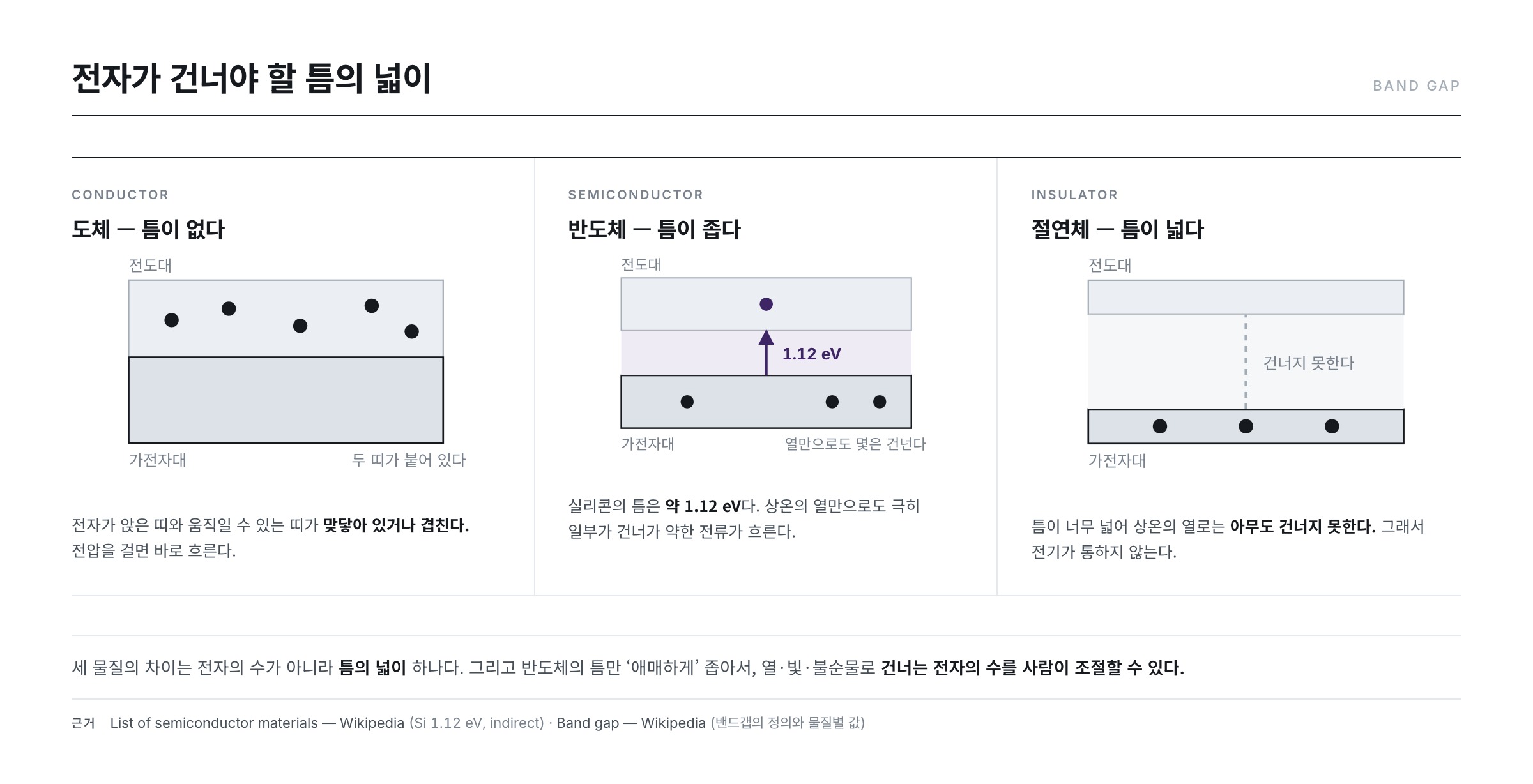
Between the two storeys is a stretch where no electron can stay. This stretch is called the band gap, the forbidden band. An electron cannot straddle this gap; it is either in the lower storey or across in the upper one.
The difference between the three kinds of matter is this one gap
In this picture the difference between conductor, semiconductor, and insulator becomes simple.
- Conductor — the two bands touch or overlap. There is no gap to cross, so apply a voltage and current flows at once.
- Insulator — the gap is too wide. Room-temperature heat gets nobody across.
- Semiconductor — the gap is awkwardly narrow. Most cannot cross, but a very few do.
The Wikipedia article "List of semiconductor materials" gives silicon's band gap as 1.12 eV. This "awkwardness" is the whole of what a semiconductor is.
Measuring just how awkward, in numbers
An eV is the energy one electron gains in crossing a potential difference of 1 V. To convert it to joules (J) you multiply by the electron charge 1.602177 × 10⁻¹⁹ C, so a band gap of 1.12 eV is 1.79 × 10⁻¹⁹ J. By the order of magnitude alone it is absurdly small, but to a single electron it is a large value. How large only shows when you set it beside the thermal energy.
The size of the energy heat gives an electron at room temperature is gauged by kT. Here k is the Boltzmann constant, 1.380649 × 10⁻²³ J/K, and T is the absolute temperature. Putting in 300 K,
kT = 1.380649 × 10-23 × 300 = 4.142 × 10⁻²¹ J
To convert to electronvolts, divide by the electron charge 1.602177 × 10⁻¹⁹ C.
kT = 4.142 × 10⁻²¹ ÷ 1.602177 × 10-19 = about 0.0259 eV
That is one forty-third of the 1.12 eV band gap. It means the average thermal energy comes nowhere close. But heat is not divided equally among all electrons. A very few are lucky enough to receive far more than the average, and those few cross the gap.
How many? The Wikipedia article "Charge carrier density" gives the intrinsic carrier concentration of silicon at 300 K as 9.65 × 109 cm-3. It means that 1 cm3 of pure silicon holds about 9.6 billion electrons that have freed themselves.
That looks like a lot until you compare. The Wikipedia article "Doping (semiconductor)" gives the number of silicon atoms in the same volume as about 5 × 10²². Dividing,
5 × 10²² ÷ 9.65 × 10⁹ ≈ 5 × 10¹²
One free electron per 5 trillion atoms. This is why pure silicon behaves effectively like an insulator.
It also explains the sensitivity to temperature. The number of electrons that cross grows exponentially with temperature. The large negative (-) temperature coefficient seen in the previous article comes out of that exponential.
So we put impurities in
If it does not conduct because it is pure, the way out is to dirty it on purpose. This operation is called doping.
N-type — an impurity that leaves an electron over
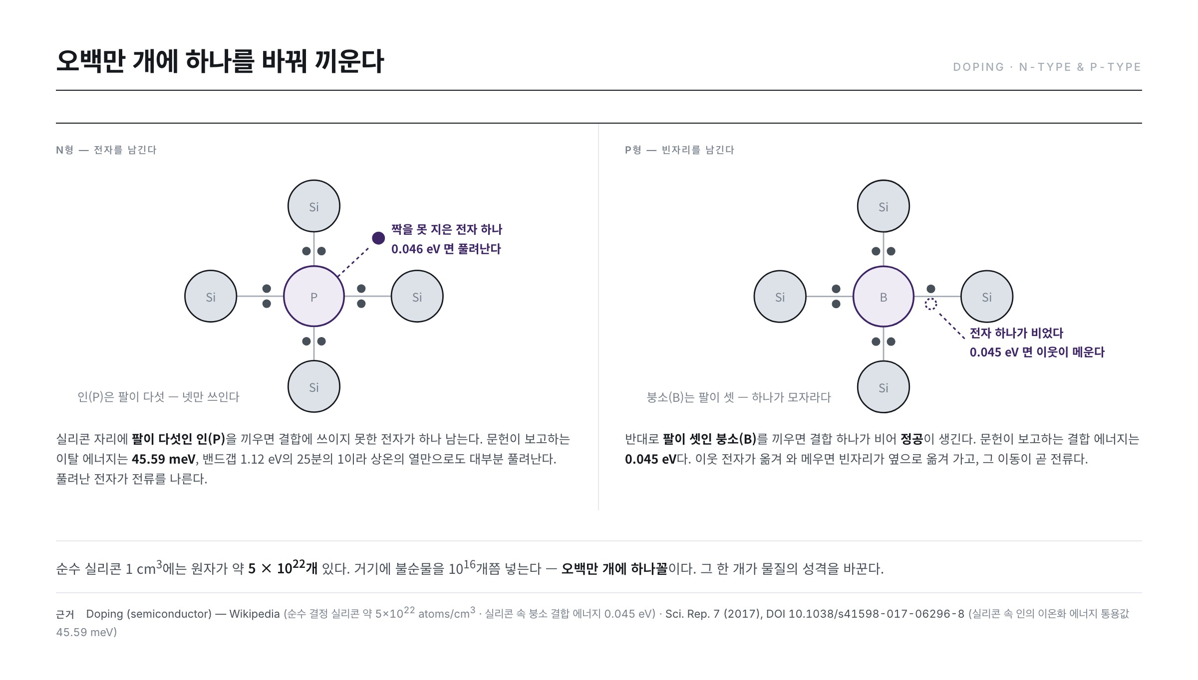
Silicon has four valence electrons. Into such a site we insert an element with five valence electrons, phosphorus (P) for instance. Four of them go into making covalent bonds with the neighbours, and one is left over.
The leftover electron is not tied into a bond, so it is held only weakly. A study published in Scientific Reports in 2017 gives the commonly used value for the ionization energy of phosphorus in silicon as 45.59 meV. That is one twenty-fifth of the 1.12 eV band gap, and dividing by the room-temperature kT of 0.0259 eV calculated above gives a mere 1.76 times.
So at room temperature nearly all of these electrons are released. Because it is an impurity that donates an electron it is called a donor, and a semiconductor in which electrons have become the majority is called N-type. The N of negative charge.
P-type — an impurity that leaves an empty place
Conversely, insert an element with three valence electrons, boron (B) for instance, and one bond ends up empty. This empty place is called a hole.
The Wikipedia article "Doping (semiconductor)" gives the binding energy of boron in silicon as 0.045 eV, set alongside a band gap of about 1.12 eV. At that level an electron from a neighbouring bond moves over easily and fills the empty place.
The moment it fills it, the place the electron left becomes the new empty place. The electron moves left, the empty place moves right, in effect. That is why a hole is treated like a particle carrying positive charge. Because it is an impurity that accepts an electron it is called an acceptor, and this semiconductor is called P-type.
How much do we put in
The "Doping (semiconductor)" article puts names to the degrees of doping. Light doping is one impurity per hundred million intrinsic atoms, heavy doping one per ten thousand, the latter written n+ and p+. It further describes that above 1018 cm-3 the material is regarded as degenerate at room temperature, behaving more like a conductor than a semiconductor, with a conductivity comparable to a metal's. These grades turn into concentrations when divided into the previous article's atomic density of 5 × 1022 cm-3.
- Light doping → 5 × 10²² ÷ 108 = 5 × 1014 cm-3
- Heavy doping → 5 × 10²² ÷ 104 = 5 × 1018 cm-3
This article will calculate assuming a doping concentration of 1016 cm-3. It lies between the two grades and is two orders of magnitude below the degeneracy line of 1018, so it is still in the stretch where the material behaves like a semiconductor. Compared with the 5 × 10²² silicon atoms,
5 × 10²² ÷ 1016 = 5 × 10⁶
One in five million. And that one raises the free electrons from 9.6 billion to 10 quadrillion — a millionfold. This is why semiconductor engineering comes down in the end to "how cleanly can you make it, and how precisely can you dirty it."
Majority and minority carriers
N-type has many electrons and P-type has many holes. The plentiful side is called the majority carrier, the scarce side the minority carrier.
A misunderstanding often arises here: imagining "many" and "few" as something like 9 to 1. The actual ratio is beyond comparison larger.
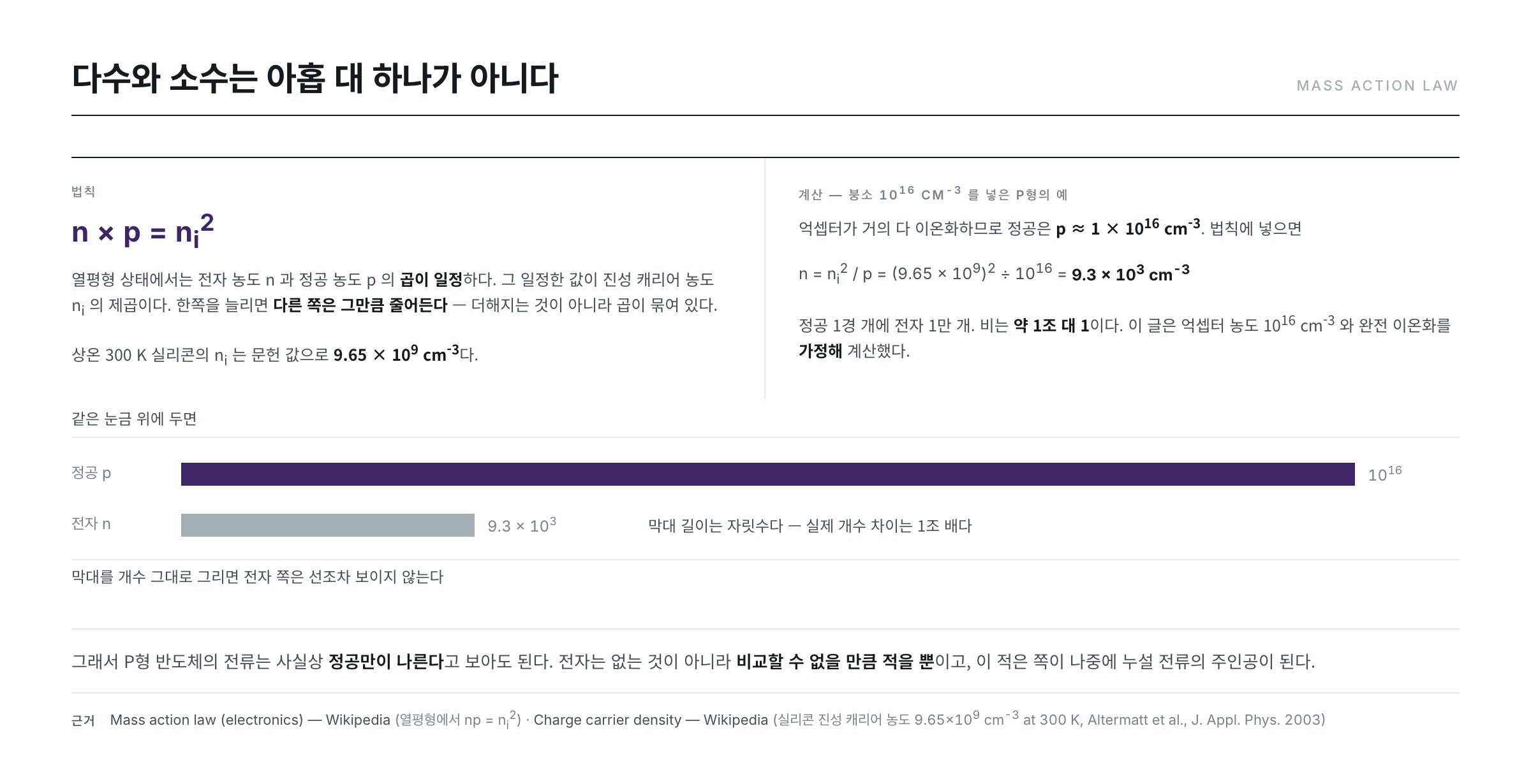
The Wikipedia article "Mass action law (electronics)" describes how, in thermal equilibrium, the product of the electron concentration n and the hole concentration p is constant at the square of the intrinsic carrier concentration.
n × p = ni2
Raise one side and the other falls by as much. They are not added; their product is pinned. Let us take as an example a P-type with 1016 cm-3 of acceptors. Assuming nearly all the acceptors ionize, p ≈ 1 × 1016 cm-3, and
n = ni2 ÷ p = (9.65 × 10⁹)2 ÷ 1016 = 9.3 × 103 cm-3
10 quadrillion holes to 9,300 electrons. The ratio is about a trillion to one. Not 9 to 1 but 1,000,000,000,000 to 1.
So it is fair to say the current in P-type is carried by holes alone, effectively. That does not make the minority carrier meaningless. The reverse leakage current of the next article is exactly what this tiny minority produces, and it is often this side that sets the performance limit of a device.
How much does doping change the resistivity
"A millionfold" does not land intuitively. Calculating it directly is quicker. The Wikipedia article "Electron mobility", quoted in the previous article, writes the conductivity as σ = e ( n μe + p μh ). Each carrier count is multiplied by its own mobility, the two are added, and the charge is multiplied in; the resistivity is its reciprocal, ρ = 1/σ. Every value to substitute has already appeared — the electron charge 1.602177 × 10⁻¹⁹ C, the mobilities μe = 1,400 and μh = 450 cm2/(V·s), and the intrinsic concentration 9.65 × 109 cm-3.
First, pure silicon. Both n and p are 9.65 × 10⁹, so
σ = 1.602177 × 10-19 × 9.65 × 109 × (1,400 + 450) = 2.86 × 10⁻⁶ S/cm
ρ = 1 ÷ (2.86 × 10⁻⁶) = 3.5 × 10⁵ Ω·cm, that is 3.5 × 10³ Ω·m
The value for pure silicon in the resistivity table quoted in the previous article was 2.3 × 10³ Ω·m. Since mobility and intrinsic concentration vary somewhat with the sample and the temperature, the same order of magnitude counts as a match.
Now N-type with 1016 cm-3 of donors. The electrons are very nearly 1016, and by the relation of the previous section the holes are 9.3 × 10³.
σ = 1.602177 × 10⁻¹⁹ × ( 1016 × 1,400 + 9.3 × 103 × 450 ) ≈ 2.24 S/cm
ρ = 1 ÷ 2.24 = 0.45 Ω·cm, that is 4.5 × 10⁻³ Ω·m
Dividing the two gives 3.5 × 10³ ÷ (4.5 × 10⁻³) ≈ 780,000 times. For the price of inserting one atom in five million, the resistivity has become one 780,000th of what it was. That is within the range the Wikipedia article "Semiconductor" writes of, that doping can change the conductivity by anywhere from thousands to millions of times.
The Fermi level — how high is it filled
There is one last concept worth taking on board: the Fermi level.
The Wikipedia article "Fermi level" defines it as the thermodynamic work required to add one electron to a solid. Intuitively, take it as the reference line showing "up to what energy the electrons are filled."
The "Fermi level" article makes one thing clear — if there is a state at the energy corresponding to the Fermi level, the probability that the state is occupied is 50%. As the conditional in that same statement, "if there is a corresponding state," reveals, there may be no state at that energy at all. That is the case in a semiconductor, where the Fermi level lies inside the band gap where no electron can stay — it is only a reference line, not a seat for an electron.
Checking that 50% against the probability formula
Where does that 50% come from? The Wikipedia article "Fermi–Dirac statistics" writes the probability that a state of energy ε is filled as F(ε) = 1 ÷ ( e(ε − μ)/kT + 1 ), where μ is the Fermi level. Put in ε = μ and the exponent becomes 0, so e0 = 1 and F = 1 ÷ (1 + 1) = 0.5.
This formula also lets us look at the situation at the bottom of the conduction band. Let us place the Fermi level at the middle of the band gap in pure silicon (an assumption of this article). The distance to the bottom of the conduction band is half the band gap, 0.56 eV, and dividing by the kT of 0.0259 eV,
(ε − μ) ÷ kT = 0.56 ÷ 0.0259 = 21.6
F = 1 ÷ (e21.6 + 1) ≈ 1 ÷ (2.4 × 10⁹) ≈ 4 × 10⁻¹⁰
It means that even where there is a state at the bottom of the conduction band, the probability of its being filled is one in 2.4 billion. The "Fermi–Dirac statistics" article writes that when (ε − μ) is far greater than kT the +1 in the denominator becomes negligible and the formula turns into the Maxwell–Boltzmann exponential form; at 21.6 we are already in that regime. What remains is a single exponential, and the temperature sits in its denominator. Raise the temperature and this probability grows exponentially — the grounds for saying earlier that the number "grows exponentially with temperature."
Doping moves this line. N-type has many electrons, so the line rises toward the conduction band; P-type has many holes, so it descends toward the valence band. The difference in the height of this line is the protagonist of the next article — what happens when N-type and P-type are pressed together and the lines sit at different heights.
Summary
- An electron can only be in the valence band or the conduction band, and cannot stay in the band gap between them. Silicon's band gap is 1.12 eV.
- The room-temperature thermal energy kT works out to about 0.0259 eV, one forty-third of the band gap. That is why only one atom in 5 trillion yields an electron that crosses on its own.
- Doping is the operation of inserting an element with 5 valence electrons (a donor, N-type) or 3 (an acceptor, P-type). Since the ionization energy is around one twenty-fifth of the band gap, nearly all of them are released at room temperature.
- The ratio of majority to minority is set by n × p = ni2. Under the example conditions it is about a trillion to one.
- Calculating with σ = e(nμe + pμh), the resistivity drops from 3.5 × 10³ Ω·m when pure to 4.5 × 10⁻³ Ω·m after doping — lower by 780,000 times.
The next article reaches the device at last. N-type and P-type are merely pressed together, and yet a wall rises at the boundary, and that one wall makes the current flow in one direction only.
References
- Electronic band structure — Wikipedia : the statement that each discrete level splits into N levels when atoms gather, the statement that N ≈ 1022 and that densely packed levels form a continuum, the statement that the Pauli exclusion principle limits an orbital to two electrons
- List of semiconductor materials — Wikipedia : silicon band gap 1.12 eV (indirect)
- Band gap — Wikipedia : the definition of the band gap — the energy stretch in which no electron can exist
- Charge carrier density — Wikipedia : intrinsic carrier concentration of silicon at 300 K, 9.65 × 109 cm-3
- Doping (semiconductor) — Wikipedia : atomic density about 5 × 10²² atoms/cm3, boron binding energy 0.045 eV, light doping one per hundred million and heavy doping one per ten thousand (n+, p+), degeneracy at room temperature above 1018 cm-3
- Scientific Reports 7, 6010 (2017) : the commonly used value of 45.59 meV for the ionization energy of the phosphorus (P) donor in silicon
- Mass action law (electronics) — Wikipedia : the relation np = ni2 in thermal equilibrium
- Electron mobility — Wikipedia : conductivity σ = e(nμe + pμh), crystalline silicon mobilities 1,400 and 450 cm2/(V·s)
- Semiconductor — Wikipedia : the statement that doping changes conductivity by anywhere from thousands to millions of times
- Fermi–Dirac statistics — Wikipedia : the occupation probability F(ε) = 1/(e(ε−μ)/kT + 1), and the statement that it reduces to the Maxwell–Boltzmann exponential form for (ε − μ) ≫ kT
- Fermi level — Wikipedia : the definition as the thermodynamic work needed to add one electron, and the 50% occupation probability where such a state exists
- CODATA — Boltzmann constant 1.380649 × 10⁻²³ J/K and elementary charge 1.602176634 × 10⁻¹⁹ C : the values substituted in the kT and eV conversions
- ※ The portions quoted from Wikipedia articles in the list above are under the CC BY-SA 4.0 licence.