The previous two articles have assembled the materials: N-type with its many electrons and P-type with its many holes. Each on its own is just a resistor. Apply a voltage and current flows; reverse the direction and it flows just the same.
And yet merely press the two together and they suddenly become something else entirely. Current flows one way and is blocked the other. Nothing further has been added.
This article looks at what happens at that boundary. Most semiconductor devices branch off from here.
The condition values in the text are examples meant to show the principle, not any particular company's specifications. Every statement quoted is one confirmed in the open literature, and the sources are listed at the end.
The moment they are joined, three things happen in turn
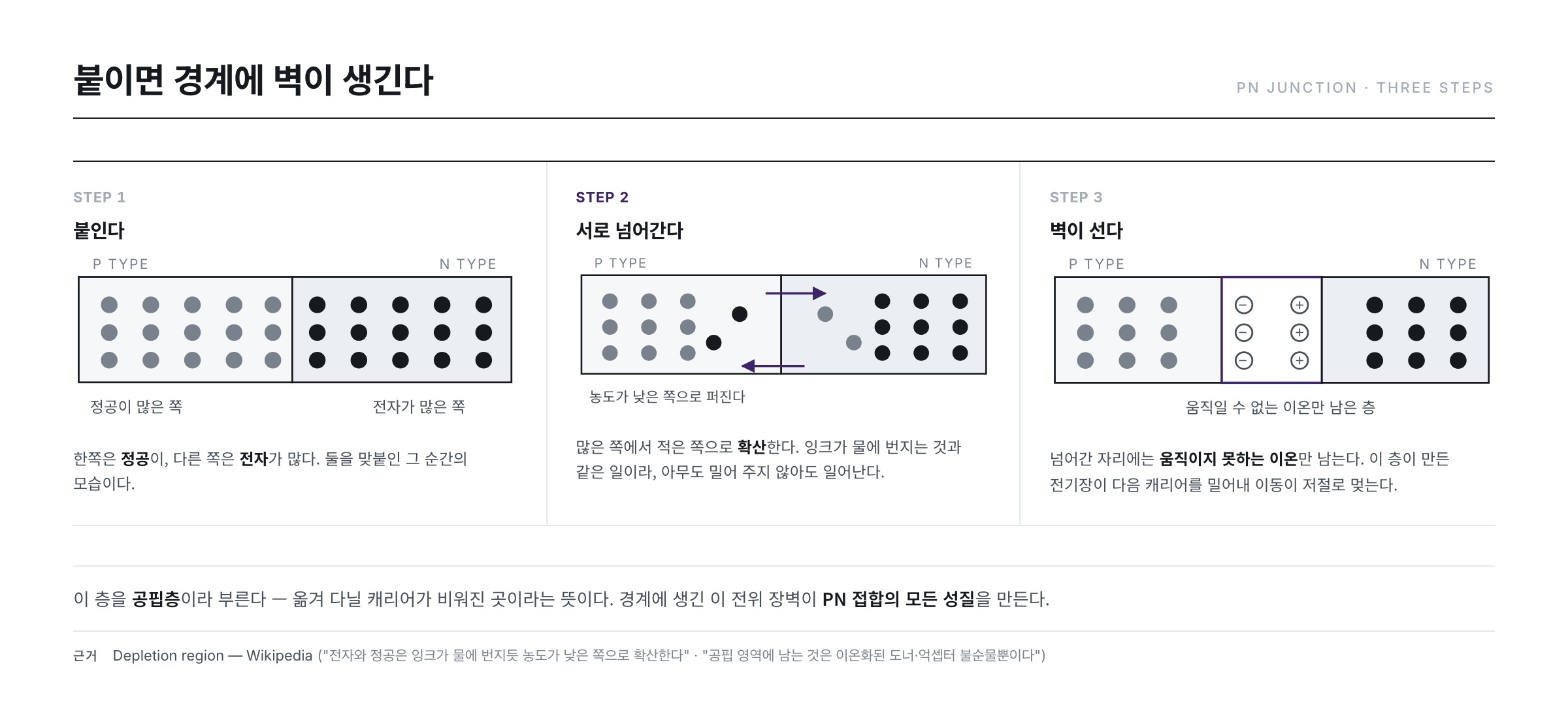
Suppose we have joined a piece of P-type and a piece of N-type at the atomic level. In practice they are made by doping a single crystal differently, but what happens is the same.
① They cross over — diffusion
The P side is dense with holes and the N side is empty of them. For electrons it is the other way round. Where the concentration is tilted, particles spread of their own accord from the crowded side to the sparse one.
The Wikipedia article "Depletion region" likens this to ink spreading in water. It happens with nobody pushing and no voltage applied. This movement is called diffusion.
It is of different parentage from the current we have handled so far. The Wikipedia article "Diffusion current" sets the two side by side and distinguishes them — drift current is the flow that arises when an electric field exerts a force on the carriers, while diffusion current is the flow that arises because the concentration is uneven, and so it flows even with no external electric field. The "Diffusion current" article writes its density as J = e De (dn/dx), where dn/dx is the concentration gradient and De is the diffusion coefficient.
The diffusion coefficient comes out of the mobility
Here a value from the previous article comes back to life. Mobility and the diffusion coefficient are not strangers. The Wikipedia article "Einstein relation (kinetic theory)" describes how, assuming a parabolic dispersion and Maxwell–Boltzmann statistics in a semiconductor, the two are tied together as D = μ kBT / q. The kBT/q at the end is the kT calculated in the previous article expressed in units of voltage, that is 0.02585 V. Let us put the previous article's mobilities straight in.
- Electrons → De = 1,400 × 0.02585 = 36.2 cm2/s
- Holes → Dh = 450 × 0.02585 = 11.6 cm2/s
The speed of being pushed along (mobility) and the quickness of spreading out (the diffusion coefficient) come out of the same number. Whatever it is that holds an electron back holds it back just the same whether it is being pushed or is spreading.
② Only immobile ions are left behind
This is the decisive point. When an electron crosses from the N side to the P side, what matters is what is left behind where it departed.
The free electron in N-type was one given up by a donor atom (phosphorus). Once the electron leaves, the phosphorus atom becomes a positive ion, and this ion is fixed in the crystal lattice and cannot move. On the P side likewise, an acceptor atom (boron) whose hole has been filled remains in place as a negative ion.
As a result a layer forms near the boundary that has no carriers left to move about, only fixed ions. The "Depletion region" article describes what remains in this region as nothing but ionized donor and acceptor impurities. In the sense that the carriers have been emptied out, it is called the depletion region.
③ It stops on its own
Positive ions line the boundary on the N side, negative ions on the P side. This arrangement creates an electric field, and its direction happens to be the one that pushes back the carriers trying to cross.
Diffusion keeps pushing and the electric field keeps pushing back. At the point where the two balance, the net movement becomes zero. The thickness of the depletion region is settled there.
"Becomes zero" does not mean nothing is happening. The "Diffusion current" article describes how, at equilibrium in a PN junction, the forward diffusion current balances the reverse drift current so that the net current is zero. The two flows merely cancel each other at equal magnitude; each is still flowing. What tips this balance is the voltage we will apply in the next section.
Nobody applied it, and yet there is a voltage
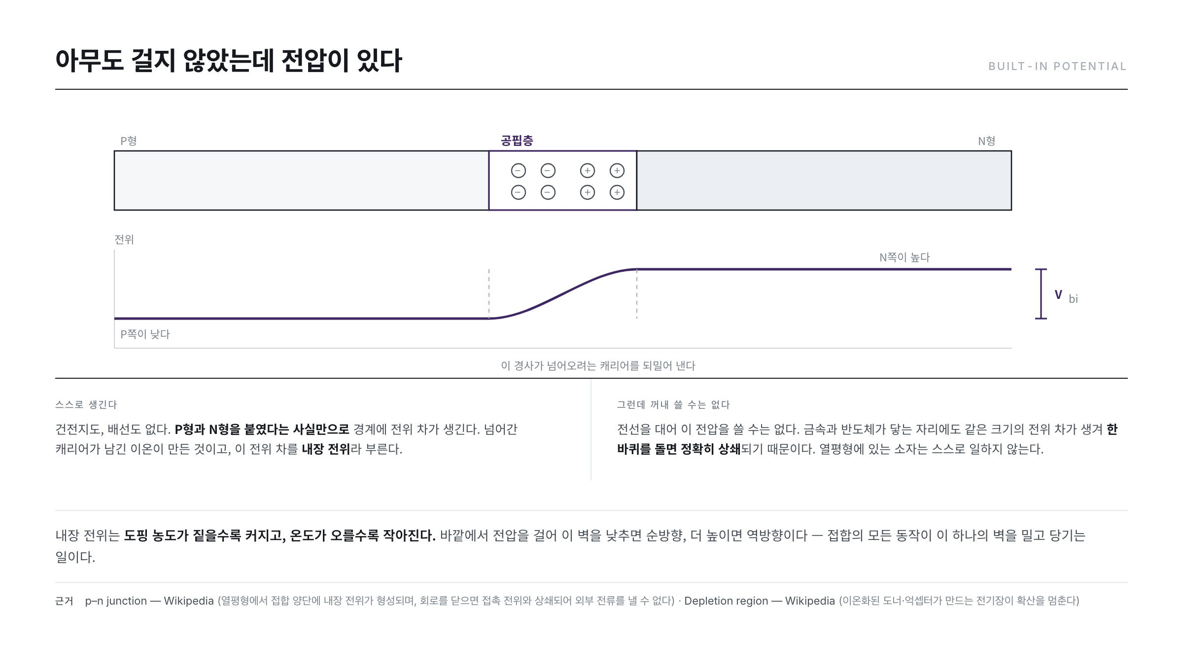
Since charge is separated across the depletion region, a potential difference arises. It is a voltage produced with no battery and no wiring, by the sole fact that two pieces were joined. This is called the built-in potential.
Here everyone thinks it once — could we not attach a wire and use this voltage?
We cannot. The Wikipedia article "p–n junction" sets down the reason. Putting a metal wire against the semiconductor creates a potential difference at that contact surface too, and going once around the circuit these cancel the built-in potential exactly. Were it otherwise, we would have a device that draws electricity out without any energy put in.
Calculating the size directly
The size need not be guessed. The Wikipedia article "p–n junction" carries the equilibrium potential of a non-degenerate semiconductor as a formula.
Vbi = (kT / q) · ln ( NA ND ÷ ni2 )
NA and ND are the doping concentrations on the two sides, ni the intrinsic carrier concentration. Let us put in the values used in the previous article — assuming both sides are doped at 1016 cm-3, with ni = 9.65 × 109 cm-3 and kT/q = 0.02585 V.
Start inside the logarithm. Since ni2 = 9.31 × 10¹⁹,
NA ND ÷ ni2 = 1032 ÷ (9.31 × 10¹⁹) = 1.07 × 10¹²
ln(1.07 × 10¹²) = 27.70
Vbi = 0.02585 × 27.70 = 0.716 V
A value slightly under 1 V. In the next article the apparent threshold voltage of a silicon diode comes out at 0.6~0.7 V, and its sitting in the same place as the wall height calculated here is no coincidence. To say a diode turns on is to say this wall has been brought almost all the way down.
Raise the doping a hundredfold and the wall rises only a little
What matters in the formula is that the doping concentration sits inside a logarithm. Let us make one side a hundred times denser, that is NA = 1018 cm-3.
NA ND ÷ ni2 = 1034 ÷ (9.31 × 10¹⁹) = 1.07 × 10¹⁴, ln = 32.31
Vbi = 0.02585 × 32.31 = 0.835 V
The concentration went up a hundredfold and the wall rose by only 0.12 V. That is how a logarithm flattens things. This is why the built-in potential of a silicon junction stays around 1 V however you set the doping. Temperature acts from the other side — kT/q grows in proportion to temperature, but as the temperature rises ni grows exponentially and shrinks what is inside the logarithm far faster, so that the wall ends up lower.
Now let us apply a voltage from outside
The workings of the device are entirely a matter of pushing and pulling this one wall.
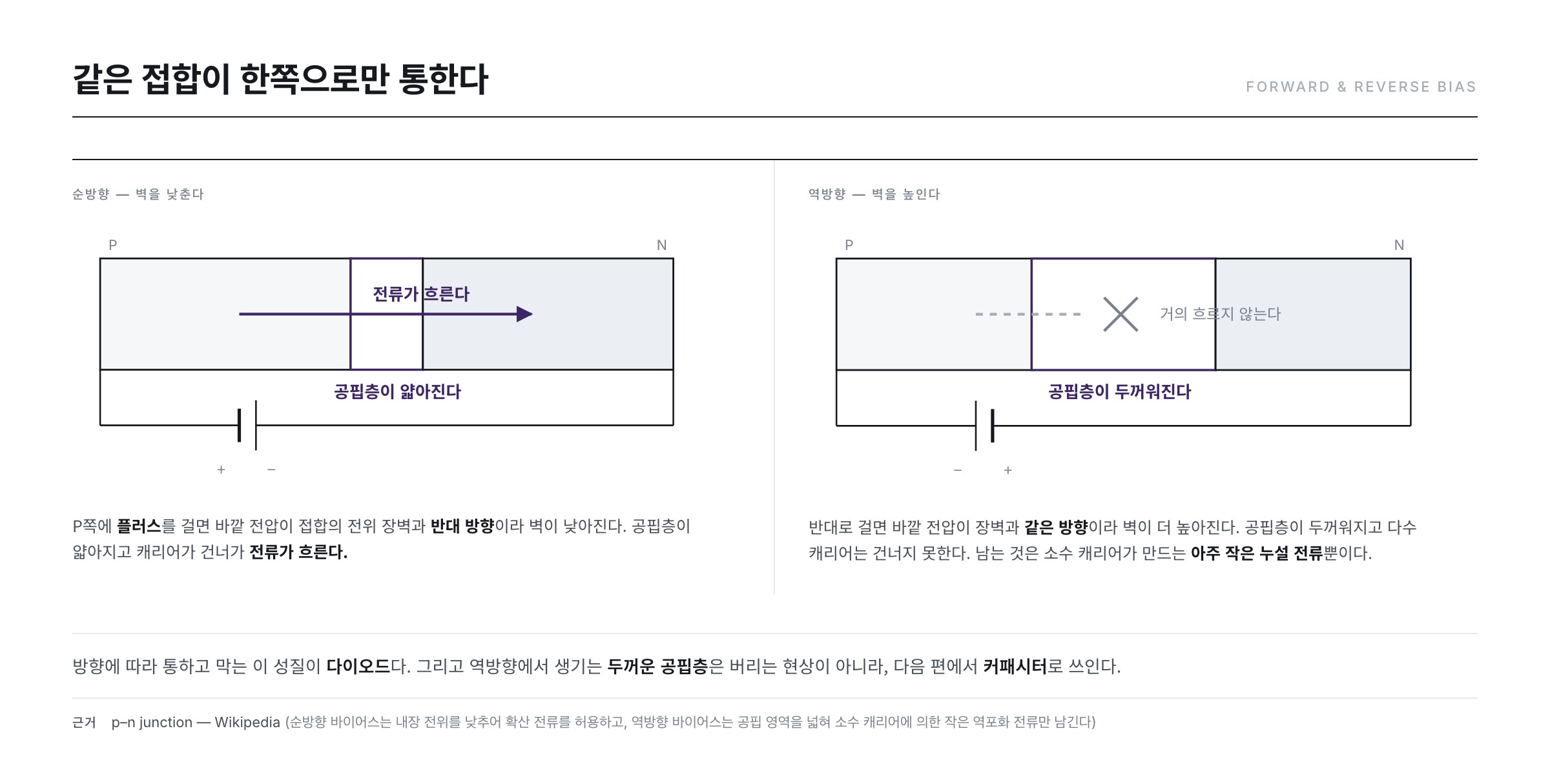
Forward — lowering the wall
Put plus on the P side and minus on the N side. The direction of the external voltage is opposite to the built-in potential, so the wall comes down.
As the wall comes down the depletion region thins, and the majority carriers that had been pushed back begin to cross. Current flows. The Wikipedia article "p–n junction" describes forward bias as lowering the built-in potential and permitting diffusion current.
Reverse — raising the wall
Applied the other way, the external voltage is in the same direction as the built-in potential, so the wall goes higher still. The depletion region thickens further, and the majority carriers cannot cross at all.
Yet the current is not exactly zero. It is time to remember the minority carriers of the previous article. Even P-type held about 9,300 electrons. For this tiny minority the raised wall is a slope they ride down instead, so they are not blocked. A very small current therefore remains, and this is the reverse saturation current, or leakage current.
The "p–n junction" article describes how, under reverse bias, only a small reverse saturation current due to minority carriers remains. Why the word "saturation" is attached becomes clear here. What sets the size of this current is not the applied voltage but how many minority carriers are generated. However much higher you raise the wall, there are only so many carriers ready to ride down it, so the current does not grow. That is why doubling or tripling the reverse voltage leaves the current all but unchanged.
And the number of minority carriers is sensitive to temperature. In the previous article we obtained the minority carrier concentration as n = ni2 ÷ p, and the numerator of that expression holds ni squared. If ni grows exponentially with temperature, its square grows twice as fast. So the leakage current grows the hotter it gets. The root of the phenomena where a screen misbehaves in a hot place lies here.
The thickness of the depletion region is set by the voltage
One more thing has to be pinned down for the next article to follow. The depletion region is not of fixed thickness.
Looking at the depletion width formula carried in the Wikipedia article "Depletion region", the width w is proportional to the square root of (Vbi − V). V is the applied voltage, and applying it in reverse flips the sign so that what is inside the parentheses grows.
- Raise the reverse voltage → the depletion region thickens. But being a square root, the voltage must go up fourfold for the thickness to double.
- Apply it forward → what is inside the parentheses shrinks, so it thins.
Measuring the thickness for real
The formula carried in the "Depletion region" article is this.
w ≈ [ 2 εr ε0 ÷ q · (NA + ND) ÷ (NA ND) · (Vbi − V) ]1/2
εr is the relative permittivity. The table in the Wikipedia article "Relative permittivity" gives silicon as 11.68, and ε0 is 8.854 × 10⁻¹² F/m. The doping on both sides is 1016 cm-3 as before, that is 1022 m-3.
The leading chunk : 2 × 11.68 × 8.854 × 10-12 ÷ (1.602 × 10⁻¹⁹) = 1.29 × 10⁹
The middle chunk : (1022 + 1022) ÷ (1022 × 1022) = 2 × 10-22 m3
Multiplying the three gives 1.29 × 109 × 2 × 10-22 × 0.716 = 1.85 × 10⁻¹³, and taking the square root,
w = 4.3 × 10⁻⁷ m, that is 430 nm
A layer about one two-hundredth the width of a hair has formed by itself, with nothing applied at all.
Now let us apply 5 V in reverse. In reverse V is negative, so what is inside the parentheses becomes 0.716 + 5 = 5.716.
1.29 × 109 × 2 × 10-22 × 5.716 = 1.48 × 10⁻¹², and the square root is 1.21 × 10⁻⁶ m, that is 1,215 nm
A full 5 V was applied and the thickness has become only 2.8 times what it was. Because 5.716 ÷ 0.716 = 7.98, and the square root of that is 2.83. This is how the words "square root" should be read.
Which side it eats into also comes out as a number
The depletion width formula in the "Depletion region" article holds the doping concentrations too. The depletion region eats deeper into the more lightly doped side. The "Depletion region" article sets down the grounds as charge balance — q NA wP ≈ q ND wN, that is, the total negative charge exposed on the P side and the total positive charge exposed on the N side must be equal. The "p–n junction" article likewise describes how, the space charge being of equal magnitude on both sides, it extends farther into the lighter side.
The charge a single ion contributes is the same on either side. So on the side where the ions are sparse, a wider stretch must be emptied to gather the same charge. Let us calculate with the asymmetric example above. With 1018 on the P side and 1016 cm-3 on the N side, Vbi is 0.835 V and the total width comes out of the depletion width formula above as 330 nm. From charge balance, wN ÷ wP = NA ÷ ND = 100, so
- Dense P side → wP = about 3 nm
- Light N side → wN = about 327 nm
Of the 330 nm, 327 nm is piled onto one side. Many drawings show the junction as symmetric, but in reality it leans like this.
The electric field inside the wall
Knowing the thickness, we can also estimate the strength of the electric field. Divide the voltage by the thickness (this article takes the field as uniform within the layer and works out only the average).
- With nothing applied → 0.716 V ÷ (4.3 × 10⁻⁷ m) = about 1.7 × 10⁶ V/m
- Reverse 5 V → 5.716 V ÷ (1.21 × 10⁻⁶ m) = about 4.7 × 10⁶ V/m
The voltage is not even 1 V, and yet the electric field is over a million volts per metre. Because the layer is that thin.
Keep raising it and it finally breaks down
So may we raise the reverse voltage without limit? The "p–n junction" article writes that once the strength of the electric field exceeds a critical level the depletion region breaks down and current begins to flow, by way of the Zener or the avalanche process. It also writes that neither process damages the device in itself.
The avalanche side is just what its name says. The Wikipedia article "Avalanche breakdown" describes how an accelerated electron or hole becomes fast enough to knock another bound electron loose, and the freed carrier does the same again, so that they multiply like an avalanche. The millions of volts per metre calculated above are that "fast enough to knock loose" electric field.
"Change the voltage and the thickness of the layer changes" — please keep that sentence well in mind. In the next article it is exactly why this junction becomes a capacitor, and the 430 nm thickness just calculated becomes the value substituted into the next article's calculation.
Summary
- Join P-type and N-type and diffusion occurs, leaving only immobile ions where the carriers crossed, which becomes the depletion region.
- The electric field those ions create stops the diffusion by itself. The potential difference left across the two ends is the built-in potential.
- The built-in potential cannot be drawn out — it cancels against the potential differences at the metal contacts.
- Forward lowers the wall and lets current flow; reverse raises the wall and blocks it, leaving only the leakage current of minority carriers.
- The built-in potential is calculated as Vbi = (kT/q)·ln(NAND/ni2), and under the example conditions comes out at 0.716 V. Raise the doping a hundredfold and it rises only 0.12 V, to 0.835 V.
- The depletion thickness is proportional to the square root of (Vbi − V). Under the same conditions it is 430 nm, and applying 5 V in reverse makes it 1,215 nm, 2.8 times as thick. Which means the thickness can be controlled by voltage.
- The layer leans toward the lightly doped side. At a hundredfold asymmetry, 327 nm of the 330 nm is on the light side.
The next article looks at how two different components come out of this one junction — the diode and the capacitor.
References
- Depletion region — Wikipedia : the ink analogy for diffusion, the statement that only ionized donors and acceptors remain in the depletion region, the depletion width formula w ≈ [2εrε0/q · (NA+ND)/(NAND) · (Vbi − V)]1/2, the charge balance qNAwP ≈ qNDwN and the statement that the depletion region leans toward the lighter side
- p–n junction — Wikipedia : the built-in potential formula (kT/q)·ln(NAND/ni2), the statement that the electric field cancels the diffusion, the statement that closing the circuit cancels it against the metal contact potentials so that no external current can be delivered, the barrier reduction under forward bias and the reverse saturation current, the statement that the space charge is of equal magnitude on both sides so it extends farther into the lighter side, the statement that beyond a critical electric field it breaks down by the Zener or avalanche process
- Diffusion current — Wikipedia : the definition of diffusion current and J = eDe(dn/dx), the contrast with drift current, the statement that at equilibrium the two cancel so that the net current is zero
- Einstein relation (kinetic theory) — Wikipedia : the statement that it reduces to D = μkBT/q in a semiconductor
- Avalanche breakdown — Wikipedia : the statement that an accelerated carrier knocks a bound electron loose and that this repeats so the carriers multiply like an avalanche
- Relative permittivity — Wikipedia : the relative permittivity table — silicon 11.68 (the value substituted in the depletion width calculation)
- Electron mobility — Wikipedia : crystalline silicon mobilities 1,400 and 450 cm2/(V·s) — the values substituted in the diffusion coefficient calculation
- Mass action law (electronics) — Wikipedia : the relation np = ni2 used in bringing over the minority carrier concentration
- Charge carrier density — Wikipedia : intrinsic carrier concentration of silicon at 300 K, 9.65 × 109 cm-3 — the value substituted in the built-in potential calculation
- ※ The portions quoted from Wikipedia articles in the list above are under the CC BY-SA 4.0 licence.