In the previous article we made a single PN junction and confirmed two things — that current flows in the forward direction and is blocked in the reverse, and that the thickness of the depletion region changes with the applied voltage.
From these two facts comes one component each, and they look nothing alike: the diode and the capacitor. This article follows both branches. And at the end it looks at how the two meet in a single pixel on a screen.
The condition values in the text are examples meant to show the principle, not any particular company's specifications. Every figure and statement quoted is one confirmed in the open literature, and the sources are listed at the end.
The diode — the component that picks a direction
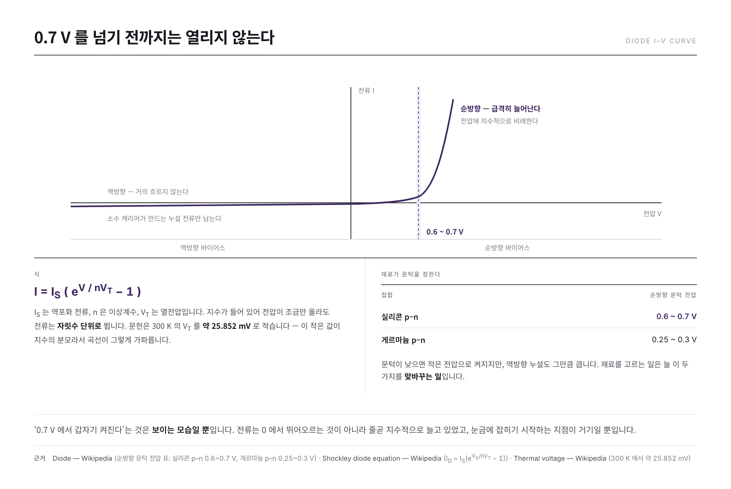
Plot the current of a PN junction against voltage and you get a curve with two utterly different halves. The left (reverse) clings to the floor, and the right (forward) shoots up almost vertically from a certain point on.
Looking at the table of forward threshold voltages carried in the Wikipedia article "Diode",
- Silicon p–n junction 0.6 ~ 0.7 V
- Germanium p–n junction 0.25 ~ 0.3 V
This is the value people who work with circuits memorize as "a silicon diode is 0.7 V."
"It switches on suddenly at the threshold" is an optical illusion
Looking at the curve, it seems a switch flicks on at 0.7 V. But the formula says otherwise.
The Wikipedia article "Shockley diode equation" writes the diode current like this.
I = IS ( eV / nVT − 1 )
IS is the reverse saturation current, n the ideality factor, and VT the thermal voltage. It contains an exponential and nothing more — there is no threshold anywhere in it. The current does not leap up from zero; it has been growing exponentially with voltage all along.
Why it looks so steep is explained by the size of VT. The Wikipedia article "Thermal voltage" gives VT at 300 K as about 25.852 mV. It is the same value as the kT of 0.0259 eV calculated in the previous article — because it is the same quantity written in units of voltage.
This small value sits in the denominator of the exponent. Every time the voltage rises by 0.0259 V the exponent grows by 1 and the current becomes about 2.7 times what it was.
For the current to become ten times as large, the exponent must grow by ln 10 = 2.303, so the voltage needed is
2.303 × 25.852 mV = about 59.5 mV
That is, a tenfold current for every 60 mV. It is the rule of thumb used most often in this article.
Putting numbers in and drawing the curve
Let us substitute directly. This article calculates assuming IS = 1 × 10-12 A and n = 1 — example values meant to show the course of the calculation, not the values of any particular component. The "Shockley diode equation" article gives the ideality factor n as lying between 1 and 2, so n = 1 is the lower end of that.
There is one more thing to drop. The "Shockley diode equation" article writes that once the forward voltage reaches a certain level the exponential term becomes far larger than 1, so that the −1 in the formula can be neglected. That leaves only I ≈ IS eV/VT. Substituting as we raise the voltage in steps of 0.1 V,
- 0.4 V → exponent 15.5, e15.5 ≈ 5.2 × 10⁶ → I ≈ 5.2 μA
- 0.5 V → exponent 19.3, e19.3 ≈ 2.5 × 10⁸ → I ≈ 0.25 mA
- 0.6 V → exponent 23.2, e23.2 ≈ 1.2 × 10¹⁰ → I ≈ 12 mA
- 0.7 V → exponent 27.1, e27.1 ≈ 5.7 × 10¹¹ → I ≈ 0.57 A
Over the 0.3 V from 0.4 V to 0.7 V, the current went from 5.2 μA to 0.57 A — 110,000 times. By the rule of thumb above, 0.3 V ÷ 59.5 mV ≈ 5, that is five orders of magnitude, so 100,000 times — the two agree.
Now it is clear why it looks like a threshold. Suppose we draw this curve on a vertical scale of 0~1 A. The 0.25 mA at 0.5 V is one four-thousandth of the scale, buried within the thickness of the line, and anything at or below 0.4 V looks glued to the floor. Then at 0.6 V and 0.7 V it suddenly surges. The device did not switch on suddenly; what came before was simply invisible. The "Diode" article likewise writes that redrawing with a logarithmic vertical axis makes the knee disappear and reveals that there is nothing special about that stretch.
Why the value stops in the reverse direction
Put a negative number into the Shockley equation and the other half of the story appears. At V = −1 V the exponent is −38.7, and e-38.7 is on the order of 10-17, effectively zero. Inside the parentheses only (0 − 1) = −1 remains, so
I ≈ −IS = −1 pA
Go further down to −2 V or −5 V and the exponential term is already zero, so the result does not change. The current does not grow though the voltage does — this is what "reverse saturation" meant in the previous article.
IS is not a fixed constant, though. The "Shockley diode equation" article writes that IS varies with temperature, and because that variation is larger than the variation of VT, a rise in temperature actually lowers the voltage needed to pass the same current. The "Diode" article likewise describes how the reverse current, in the microampere range, can climb to milliamperes and beyond once the temperature is high enough.
This left-right asymmetry is the usefulness of the diode itself. The "Diode" article writes that this property of flowing in one direction only is used to turn alternating current into direct current, and that this is called rectification.
The low threshold of germanium in the table is the same story. Its band gap is narrow, so far more current flows at the same voltage and it registers on the scale earlier. But for that same reason its reverse leakage is large as well. Lowering the threshold and reducing the leakage are always in a relation of trade-off.
The capacitor — using the blocking layer the other way round
Now the other side. When we have applied a reverse voltage and blocked the current, what has that device become?
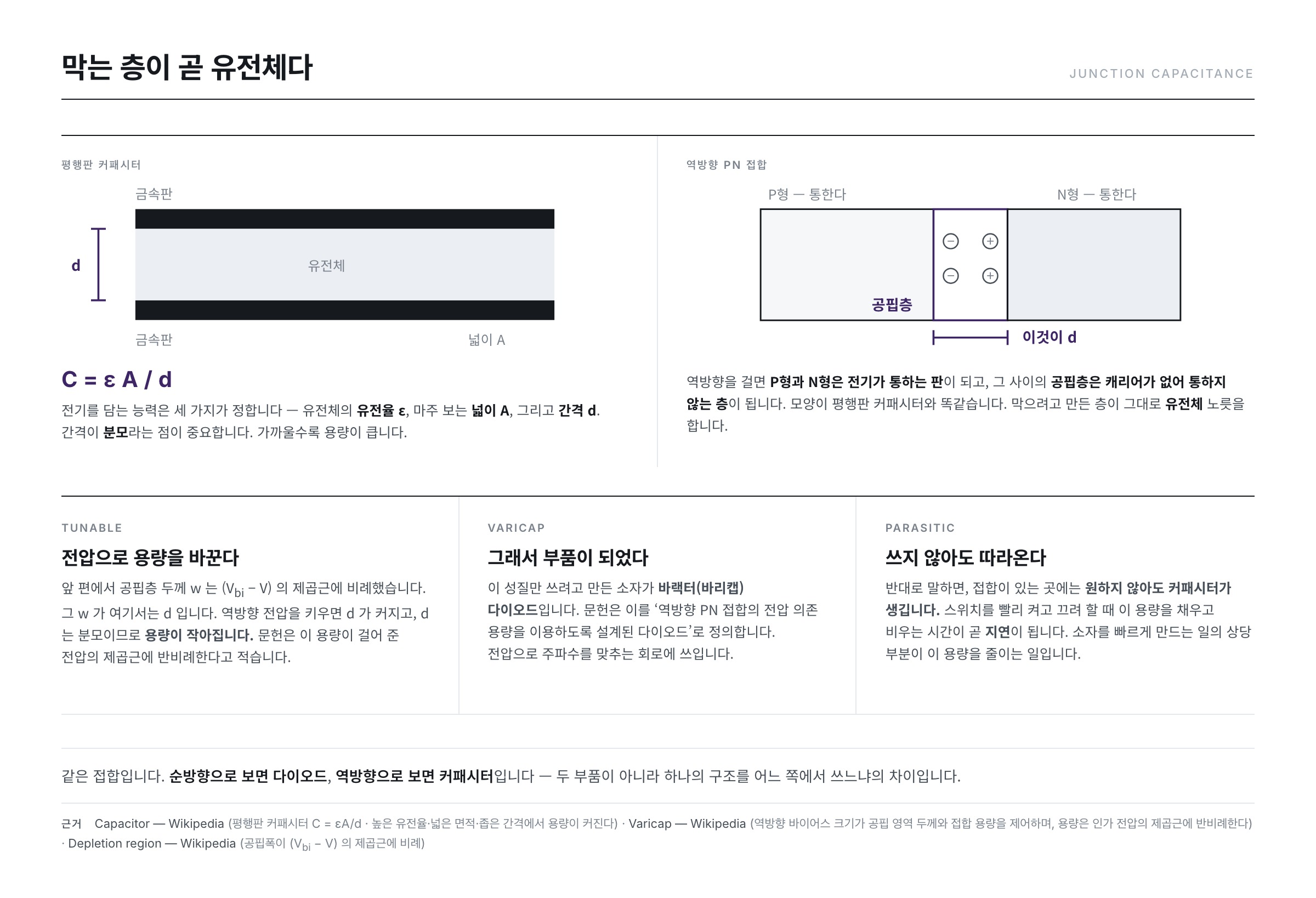
A capacitor is a component that holds electricity. Its simplest form is two metal plates with a non-conducting material sandwiched between them. The Wikipedia article "Capacitor" defines capacitance as C = Q / V, the ratio of the charge Q carried on the two conductors to the voltage V between them. Hold more charge at the same voltage and the capacitance is larger.
If the plates are flat and parallel, the shape sets the capacitance. The "Capacitor" article writes the capacitance of a parallel-plate capacitor like this.
C = ε A / d
ε is the permittivity of the sandwiched material, A the facing area, d the spacing. The "Capacitor" article describes the capacitance as growing the higher the permittivity, the wider the area, and the narrower the spacing. Please keep in mind that the spacing is in the denominator.
Let us look at the reverse-biased PN junction again.
- The P-type region — many holes, so it conducts. That is one plate.
- The N-type region — many electrons, so it conducts. That is the other plate.
- The depletion region between them — no carriers to move about, so it does not conduct. That is the sandwiched dielectric.
The shape is exactly a parallel-plate capacitor. The layer that formed in order to block current serves as the dielectric just as it is. This capacitance is called the junction capacitance.
Changing the capacitance with voltage
Here the last sentence of the previous article comes alive. The depletion thickness was proportional to the square root of (Vbi − V). That thickness is, here, d.
Raise the reverse voltage and d grows. Since d is in the denominator, the capacitance falls. The Wikipedia article "Varicap" puts this in two sentences — the magnitude of the reverse bias controls the thickness of the depletion region and the junction capacitance, and the capacitance is inversely proportional to the square root of the applied voltage.
A capacitor whose value can be changed by voltage makes a component. The "Varicap" article defines the varactor (varicap) diode as a diode designed to exploit the voltage-dependent capacitance of a reverse-biased PN junction. The circuits that tune a radio's frequency by voltage rather than by a knob use this.
Put the numbers in and out comes the picofarad range
In the previous article we actually calculated the thickness of the depletion region. It was 430 nm with nothing applied and 1,215 nm under 5 V in reverse. Put those values straight into the place of d here and the capacitance comes out.
The permittivity is ε = εr ε0. Multiplying the silicon relative permittivity of 11.68 from the Wikipedia article "Relative permittivity" by ε0 = 8.854 × 10⁻¹² F/m,
ε = 11.68 × 8.854 × 10-12 = 1.03 × 10⁻¹⁰ F/m
For the area we will assume a 100 μm square, that is A = 10-8 m2. Now to substitute.
- With no voltage applied → C = 1.03 × 10-10 × 10-8 ÷ (4.3 × 10⁻⁷) = 2.4 pF
- Reverse 5 V → C = 1.03 × 10-10 × 10-8 ÷ (1.215 × 10⁻⁶) = 0.85 pF
These fall within the 1~10 pF the "Varicap" article gives as the capacitance range of early varicaps. That a 100 μm square yields this much capacitance is because d is on the nanometre scale.
How much must we apply to halve the capacitance? d must double, and since d is the square root of (Vbi − V), what is inside the parentheses must become four times larger.
Vbi − V = 4 × 0.716 = 2.864 → V = 0.716 − 2.864 = −2.15 V
At 2.15 V in reverse the capacitance halves. The "Varicap" article names voltage-controlled oscillators and frequency synthesizers as circuits that use this property, and writes that it serves to tune the frequency of radios, televisions, and mobile phones.
It comes along whether you use it or not
Turned around, it becomes a more important fact. Wherever there is a junction, a capacitor appears whether you want it or not.
Every time the switch turns on and off, this capacitance must be filled and emptied. That time is precisely delay.
How long it takes can be calculated too. The "Capacitor" article writes that when charging through a resistance the voltage follows V(t) = V0(1 − e−t/τ) and that τ = RC is its time constant. Taking 2.4 pF and assuming a wiring resistance of 1 kΩ,
τ = 103 × 2.4 × 10-12 = 2.4 × 10⁻⁹ s, that is 2.4 ns
To fill to 99% of the target voltage, e−t/τ must become 0.01, so t = τ × ln 100 = 4.6τ, which takes about 11 ns. This is why much of the work of making a device fast is not raising its performance but reducing this capacitance that tags along.
Seen from the holding side, that same capacitance is an asset. Putting 2.4 pF and 5 V into the stored energy W = ½ C V2 given in the "Capacitor" article gives 3.0 × 10⁻¹¹ J, that is 30 pJ. The same component is both a burden that slows the signal and a vessel that holds the value.
The choice of material hangs on this as well. The table in the "Relative permittivity" article gives the relative permittivity of silicon as 11.68 and that of silicon dioxide as 3.9. A threefold difference. Where you want to hold charge you use a material of high permittivity; where you want to reduce the capacitance that tags along, a low one.
The two meet in a pixel on a screen
Let us finish by looking at just one place where the components we have arrived at live: a single pixel of a liquid-crystal screen.
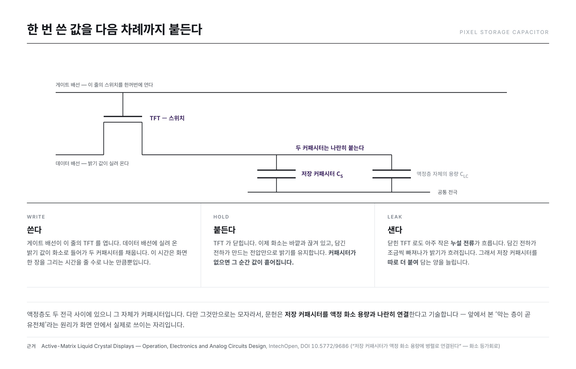
The screen is drawn a line at a time. The Wikipedia article "Thin-film-transistor liquid-crystal display" describes how the pixels are addressed by row and column, reducing millions of connections to thousands, with the row and column lines running to a transistor switch attached one per pixel. When a gate line opens a whole row of switches at once, the brightness values carried on the data lines enter the pixels of that row. Then the switches close.
The problem is what comes next. After the switch closes, the pixel is cut off from the outside until its turn comes round again, and to hold its brightness in the meantime the value must be stored somewhere.
Let us first see how long that is. The Wikipedia article "Refresh rate" defines the refresh rate as how many times per second the display shows a new image, and writes that liquid-crystal monitors are often fixed at 60 frames per second. Dividing by 60, one frame is about 16.7 ms, and a single pixel must hold its value alone for that long.
The liquid-crystal layer itself sits between two electrodes, so it too is a capacitor. The "Refresh rate" article writes that, unlike a cathode-ray tube, a pixel of a liquid-crystal screen holds its state as long as power is supplied. But that alone does not hold enough. A very small leakage current flows even through a closed switch, and the stored charge drains away little by little so the brightness fades.
How much it fades comes out of turning the earlier C = Q/V around. If the charge drains by ΔQ the voltage falls by ΔQ/C, and if a leakage current I flows for Δt then ΔQ = I·Δt, so
ΔV = I × Δt ÷ C
We will assume a leakage current of 1 pA and take the capacitance as the 2.4 pF calculated above (both are example values meant to show the calculation).
ΔV = 10-12 × 16.7 × 10-3 ÷ (2.4 × 10⁻¹²) = about 7 mV
Seven millivolts slide away over one frame. If the capacitance were only a tenth of that, 0.24 pF, the same calculation drains 70 mV. Because C is in the denominator. The larger the vessel, the less the reading moves for the same amount leaked.
So one more capacitor is added. The commentary on active-matrix liquid-crystal displays published by IntechOpen (DOI 10.5772/9686) describes the pixel equivalent circuit and states that a storage capacitor is connected in parallel with the liquid-crystal pixel capacitance.
To sum up, a single pixel is this.
- A switch — it decides when to write. This is the thin-film transistor.
- A capacitor — it holds the written value until the next turn.
The "Thin-film-transistor liquid-crystal display" article also writes that thanks to the transistor's property of passing current in one direction only, the charge placed on a pixel does not drain away between refreshes. That is what the diode's one-way property, which we have just been handling, does inside a screen. And it describes the amorphous silicon thin-film transistor as the most widely used material for making that switch — the very material whose mobility was said to be about 1 in article 1.
Every principle we have seen so far is contained in this small rectangle. There is a junction, there is a depletion region, there is a leakage current, and there is a layer that holds charge.
Summary
- The current of a diode has no threshold. It is simply an exponential, and because the thermal voltage in the denominator is a small 25.852 mV or so, it grows tenfold every 60 mV and thus looks like a threshold. Silicon's apparent threshold is 0.6~0.7 V.
- Putting in the example values gives 5.2 μA at 0.4 V and 0.57 A at 0.7 V, a difference of 110,000 times. The scale simply fails to show what came before.
- A reverse-biased junction is a capacitor. P-type and N-type are the plates, the depletion region is the dielectric, and the capacitance follows C = εA/d.
- Since the reverse voltage sets the spacing, the capacitance is tuned by voltage — the component built solely around that is the varactor diode.
- Putting in the previous article's depletion width of 430 nm and a 100 μm square gives a junction capacitance of 2.4 pF, and 0.85 pF under 5 V in reverse. The reverse voltage needed to halve the capacitance is 2.15 V.
- Conversely, wherever there is a junction an unwanted capacitance tags along, and it limits the speed of the device. With 2.4 pF and 1 kΩ, τ = RC = 2.4 ns, and filling to 99% takes about 11 ns.
- A single liquid-crystal pixel is made of one switch and a capacitor.
That is the opening stretch of this series. We started from the material, passed through the junction, and arrived at components. Next we move on to a device with not two terminals but three — the transistor, which does not switch a flow on and off but regulates it.
References
- Diode — Wikipedia : forward threshold voltages — silicon p–n 0.6~0.7 V, germanium p–n 0.25~0.3 V; the statement that drawing the vertical axis logarithmically makes the knee disappear; the statement that the one-way characteristic is rectification; the statement that the reverse current grows to milliamperes and beyond at high temperature
- Shockley diode equation — Wikipedia : ID = IS(eVD/nVT − 1) and the definition of each term, the statement that the ideality factor n is 1~2, the statement that the −1 can be neglected in the forward direction, the statement that IS varies more with temperature than VT does
- Thermal voltage — Wikipedia : the definition VT = kT/q, about 25.85 mV at 300 K
- Capacitor — Wikipedia : C = Q/V, the parallel plate C = εA/d and the statement that capacitance is greatest with high permittivity, wide area, and narrow spacing, the stored energy W = ½CV2, the time constant τ = RC and the charging law V(t) = V0(1 − e−t/τ)
- Varicap — Wikipedia : the statement that the reverse bias controls the depletion thickness and the junction capacitance and that the capacitance is inversely proportional to the square root of the applied voltage, the definition of the varactor, the early varicap capacitance of about 1~10 pF, the use in voltage-controlled oscillators and frequency synthesizers
- Depletion region — Wikipedia : the relation that the depletion width is proportional to the square root of (Vbi − V) — the source of the thickness used in the capacitance calculation
- Relative permittivity — Wikipedia : the relative permittivity table — silicon 11.68, silicon dioxide 3.9
- Refresh rate — Wikipedia : the definition of refresh rate, the statement that liquid-crystal monitors are usually fixed at 60 frames per second, the statement that a liquid-crystal pixel holds its state as long as power is supplied
- Thin-film-transistor liquid-crystal display — Wikipedia : row and column addressing and the transistor switch attached to each pixel, the statement that the transistor's one-way characteristic prevents charge loss between refreshes, the statement that the amorphous silicon TFT is the most widely used
- Active-Matrix Liquid Crystal Displays, IntechOpen (DOI 10.5772/9686) : the statement that in the pixel equivalent circuit a storage capacitor is connected in parallel with the liquid-crystal pixel capacitance
- ※ The portions quoted from Wikipedia articles in the list above are under the CC BY-SA 4.0 licence.