Let us count what the previous four installments built. There was a silicon crystal; impurities were added to it to obtain N-type and P-type; the two were joined into a PN junction. Out of that single junction came the diode and the capacitor.
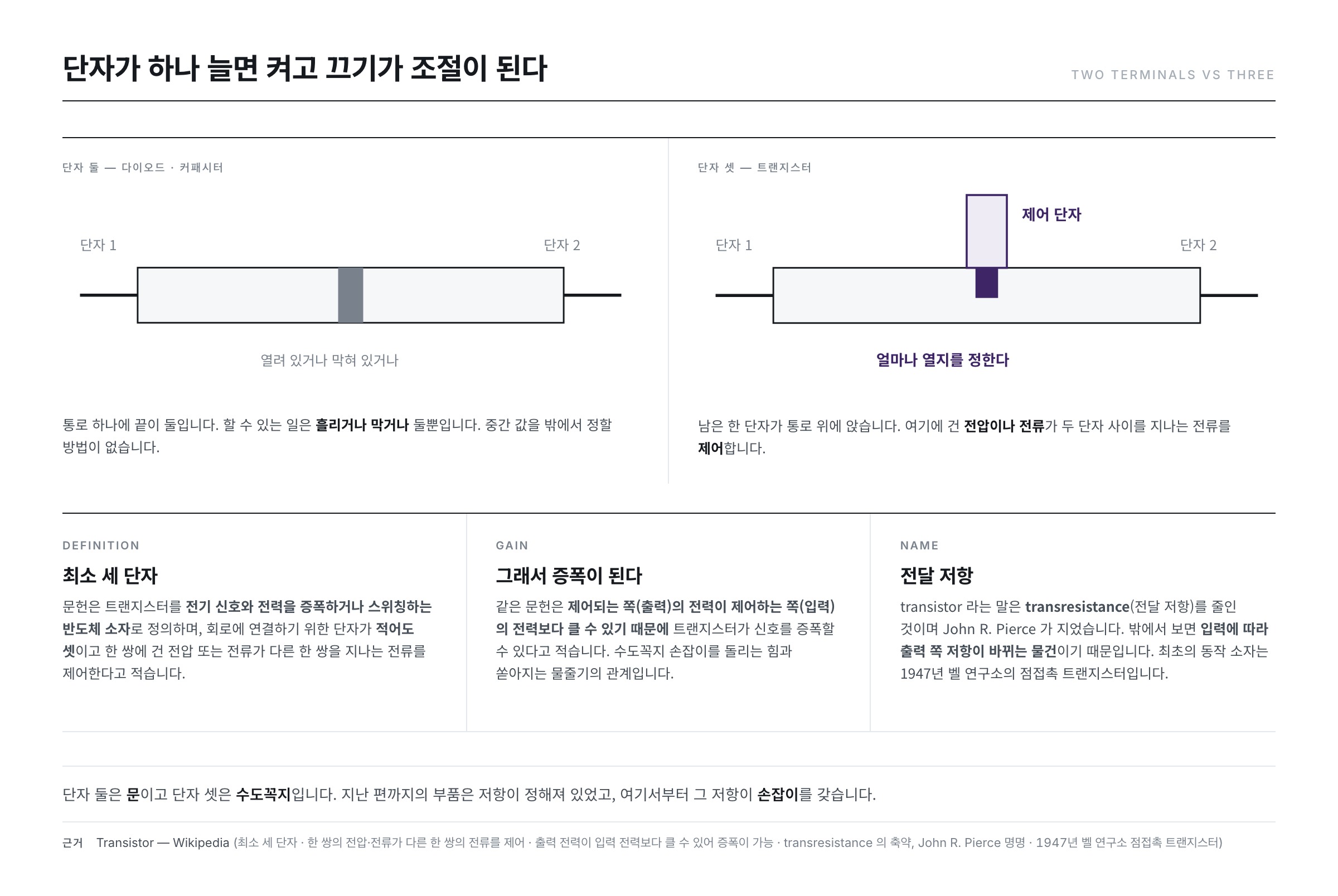
Every component so far has two terminals. With two terminals, what a device can do is already settled. It either passes current or blocks it — one of the two. It opens and closes a door.
In this installment we attach one more terminal. The character of the device changes completely. Instead of opening and closing, it becomes possible to decide how far to open. That is the transistor, and this installment looks at its first form, the bipolar junction transistor (BJT).
The operating values in this text are examples meant to show how a calculation goes, not the specifications of any particular company. Every figure and statement quoted here was confirmed in published literature, and the sources are listed at the end.
What It Means to Have Three Terminals
The Wikipedia "Transistor" article defines the transistor this way — it is a semiconductor device used to amplify or switch electrical signals and power, it has at least three terminals for connection to a circuit, and a voltage or current applied to one pair of terminals controls the current through another pair.
That last clause is the heart of it. Three terminals means "two plus one." The path the current takes lies between two terminals, and the remaining one controls that path.
A water tap is a close picture. There is a side the water comes in and a side it goes out, and the handle is separate. The force needed to turn the handle is small, but the stream it regulates is large. The "Transistor" article makes this point explicitly — because the power of the controlled side (the output) can be greater than the power of the controlling side (the input), a transistor can amplify a signal.
The name came from here as well. The "Transistor" article notes that the word transistor is a contraction of transresistance and that it was coined by John R. Pierce. The first working device was the point-contact transistor built in 1947 at Bell Labs by John Bardeen, Walter Brattain and William Shockley.
It is worth noticing that "resistance" sits inside the name. Seen from the outside, this three-terminal device looks like a thing whose output-side resistance changes according to the input-side signal. The components of the earlier installments had a fixed resistance; now that resistance has been given a handle.
The Structure of a BJT — There Are Two Junctions
The Wikipedia "Bipolar junction transistor" article defines the BJT as a transistor that uses both electrons and holes as charge carriers. The name "bipolar" comes from this: the carriers are not of one kind but of two.
The structure is three differently doped regions — emitter, base and collector — and between those three arise two PN junctions. The junction we have handled so far has simply gone from one to two; that is the whole of the structure.
If the doping order is N-P-N it is an NPN; if P-N-P, a PNP. The middle layer is the base.
- Emitter — the side that injects carriers.
- Base — the thin middle layer. Control happens here.
- Collector — the side that collects the carriers that made the crossing.
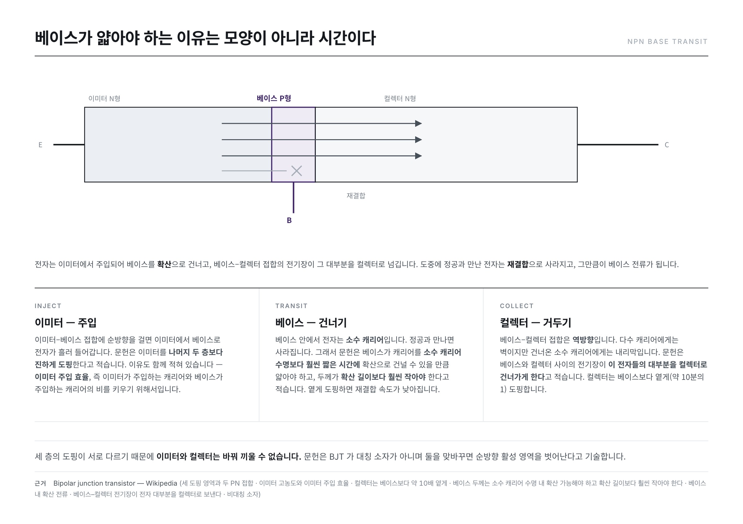
The three regions differ in doping concentration. The literature states that the emitter is heavily doped compared with the other two layers, and the collector is doped more lightly than the base (roughly one tenth). The reason for doping the emitter heavily is given alongside — emitter injection efficiency, that is, to increase the ratio between the carriers the emitter injects and those the base injects. Injection has been arranged so that the emitter does nearly all of it alone.
Because of this asymmetry, emitter and collector cannot be swapped. The literature describes the BJT as, unlike some other transistors, not a symmetric device: exchanging collector and emitter takes it out of the forward-active region. Even when the two outer layers look alike in a diagram, they are not the same thing.
Why the Base Must Be Thin
The heart of the BJT is contained in that one base layer.
Take the NPN as the example. Apply a forward voltage to the emitter–base junction and that junction becomes forward-biased, and, as the literature describes, electrons flow from the emitter into the base. This is the same behaviour as the diode of the previous installment.
The question is what happens next. The base is P-type, and there the electrons are minority carriers. Electrons have entered a place full of holes. These electrons diffuse from the emitter side, where their concentration is high, toward the collector side, where it is low. The literature calls this flow a diffusion current across the base. If an electron meets a hole on the way, it recombines and disappears.
An electron that crosses safely reaches the base–collector junction. That junction is reverse-biased. But a reverse-biased junction is not a wall to a minority carrier; it is a downhill slope. The literature states that the electric field existing between base and collector sweeps most of these electrons across into the collector. That is the collector current.
So the performance of this device is settled by how many electrons cross the base without disappearing. The literature sets out the conditions in three lines.
- To reduce the carriers that recombine before reaching the collector–base junction, the base must be thin enough that carriers can diffuse across it in far less time than the minority carrier lifetime.
- In particular, the base thickness must be much less than the diffusion length of the carriers.
- Light doping of the base lowers the recombination rate.
"The base is thin" is therefore not a statement about shape. It is a statement about time. The electron must reach the far side before it disappears, and that limit sets the thickness. For the same reason the base cannot be heavily doped: heavy doping means more holes to meet, and so more electrons lost on the way.
β — A Small Current Makes a Large One
Now let us put a number on how much gain this structure gives. The literature defines two current gains.
αF = IC / IE — the common-base current gain. It is the fraction of the current leaving the emitter that reaches the collector. The literature states that this value is close to 1 and lies between 0.980 and 0.998.
βF = IC / IB — the common-emitter current gain. This is the value written as hFE in component datasheets. The literature states that for small-signal transistors this value is greater than 50.
The currents at the three terminals are bound together. The literature states that the emitter current is the sum of the other two — IE = IB + IC. With this one line the two gains can be written in terms of each other.
β = IC / IB = IC / (IE − IC) = α / (1 − α)
The "Bipolar junction transistor" article carries this relation as it stands. Let us substitute the range of α above into it. The values substituted are the two ends of the range the literature gives, and its middle.
- α = 0.980 → β = 0.980 / 0.020 = 49
- α = 0.990 → β = 0.990 / 0.010 = 99
- α = 0.998 → β = 0.998 / 0.002 = 499
These three lines are the most striking passage in this installment. α rose from 0.980 to 0.998 — by less than two per cent. Yet β went from 49 to 499, a factor of ten.
This is because the denominator is (1 − α). As α approaches 1 the denominator approaches 0 and the quotient grows steeply. What sits in the denominator is the remainder that failed to cross the base. What settles the gain is not the side that crossed but the side that did not.
The discussion of the base in the previous section leads here. Making the base thin and lightly doped is the work of pushing α up from 0.98 toward 0.998. That minute difference changes the gain by a factor of ten. Conversely, if the base is thick, more electrons disappear on the way, the denominator grows, and the gain collapses.
The identity of the base current also becomes clear. The base current is the share lost to recombination plus the share the base injects back. Saying that β is 99 means "at the cost of losing 1, it delivers 99." It looks as though the small current fed into the base terminal creates the large current at the collector, but what actually happens is that it makes up for what leaks out of a large flow.
Three Operating Regions
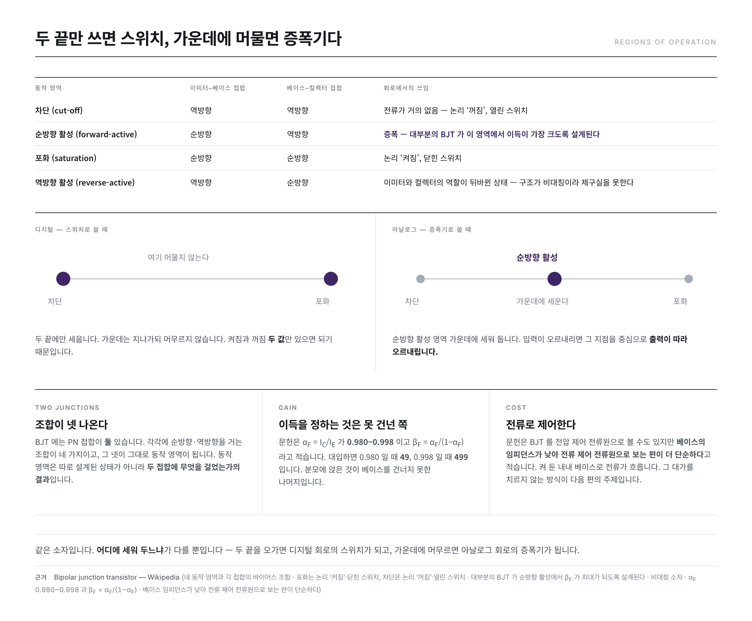
Since there are two junctions, forward and reverse bias combine into four cases at the two junctions. This is exactly as the literature sets them out.
- Cut-off — both junctions reverse-biased. The literature states that almost no current flows and that this corresponds to logic "off," that is, an open switch.
- Forward-active — emitter–base forward, base–collector reverse. This is the behaviour we followed above. The literature states that most BJTs are designed so that βF is greatest in this region. It is the region of amplification.
- Saturation — both junctions forward-biased. The literature states that this corresponds to logic "on," that is, a closed switch.
- Reverse-active — emitter–base reverse, base–collector forward. The roles of emitter and collector are exchanged. Because the structure is asymmetric, the device does not perform properly in this direction.
Here the two faces of this device part ways.
- Used as a switch, only cut-off and saturation are used — the two ends only. The middle is passed through but not dwelt in. Digital circuits use it this way.
- Used as an amplifier, it is parked in the middle of the forward-active region. As the input rises and falls, the output rises and falls about that point. Analogue circuits use it this way.
It is the same device. Only where it is parked differs.
The Price of Controlling with Current
One thing has lain beneath the whole discussion so far. To keep a BJT turned on, current must keep flowing into the base. The literature states that although the BJT can be viewed as a voltage-controlled current source, because the impedance at the base is low it is simpler to treat it as a current-controlled current source, that is, a current amplifier.
Current flowing means power being spent. Even with β of 99, passing 1 A through the collector requires about 10 mA to be pushed continuously into the base. It stays that way the whole time the device is on. For a single device this hardly matters. Put hundreds of millions of them on the same piece of silicon and the story changes.
There is another way. Control by electric field instead of by current. The Wikipedia "Field-effect transistor" article defines the FET (field-effect transistor) as a transistor that uses an electric field to control the current through a semiconductor. Even the terminal names are different — the source, where carriers enter, the drain, where they leave, and the gate, which changes the conductivity of the channel. The "Field-effect transistor" article states that applying a voltage to the gate changes the conductivity between drain and source.
The difference from the BJT lies in two places.
- The number of carrier types — the "Field-effect transistor" article calls the FET a unipolar transistor, because it uses only one of electrons (N-channel) or holes (P-channel), not both. This is exactly the opposite of the BJT, which uses both kinds. The names "bipolar" and "unipolar" part ways here.
- The price of control — the "Field-effect transistor" article states that the FET shows very high input impedance at low frequencies. That means almost no current flows through the control terminal. Holding the handle costs no effort.
What that difference changes is the subject of the next installment. The "Field-effect transistor" article distinguishes devices in which a channel already exists at a gate voltage of 0 from those in which it does not, calling the former depletion mode and the latter enhancement mode. That distinction is also taken up next time.
Summary
- With three terminals, a voltage or current applied to one pair controls the current through the other pair. Because the output power can exceed the input power, this becomes amplification.
- A BJT is three differently doped regions and two PN junctions. The emitter is doped heavily, the base lightly and thinly, the collector more lightly still.
- The reason the base must be thin is time. Carriers must cross in far less time than the minority carrier lifetime, and the thickness must be much less than the diffusion length.
- Since β = α / (1 − α), when α rises from 0.980 → 0.998, β becomes 49 → 499. What settles the gain is the side that did not cross.
- The bias combinations of the two junctions produce cut-off, forward-active and saturation. Use only the two ends and it is a switch; stay in the middle and it is an amplifier.
A BJT keeps eating current the whole time it holds the handle. In the next installment we move on to a way of controlling that does not pay that price — the field-effect transistor (FET), which changes the width of the channel with an electric field.
References
- Transistor — Wikipedia : the definition of the transistor (amplifying and switching, at least three terminals, a voltage or current at one pair controlling the current at another pair), the statement that the output power can exceed the input power so that amplification results, the statement that the word is a contraction of transresistance coined by John R. Pierce, the 1947 Bell Labs point-contact transistor
- Bipolar junction transistor — Wikipedia : the definition of using both electrons and holes, three doped regions and two PN junctions, heavy emitter doping and light collector doping (about one tenth that of the base) together with emitter injection efficiency, the conditions on base thickness (minority carrier lifetime, diffusion length), the diffusion current within the base, the statement that the field at the reverse-biased junction sweeps most carriers into the collector, αF = IC/IE (0.980~0.998) · βF = IC/IB (greater than 50 for small signal) · βF = αF/(1−αF) · IE = IB + IC, the bias combinations of the four operating regions and the correspondence of saturation and cut-off to logic on and off, the statement that it is not a symmetric device, the statement that it is simpler to view it as a current-controlled current source
- Field-effect transistor — Wikipedia : the definition of controlling current with an electric field, the roles of source, drain and gate, the description as a unipolar transistor (using only one carrier type, electrons or holes), very high input impedance at low frequencies, the distinction between depletion mode and enhancement mode
- ※ The portions quoted above from Wikipedia articles are licensed under CC BY-SA 4.0.