In the previous installment we set up a current equation. It said that once the gate voltage crosses the threshold a channel forms, and that raising the drain voltage increases the current until, past pinch-off, it flattens out.
That equation had a premise lying quietly underneath it: that the channel is long enough. Long and short only hold as terms if there is a ruler to compare against, and that ruler is the thickness of the depletion layers formed around the source and drain.
The Wikipedia "Short-channel effect" article defines short-channel effects as phenomena appearing in MOSFETs in which the channel length has become comparable to the depletion-layer thickness of the source and drain junctions. This installment follows where the previous installment's equation begins to go wrong at that point.
The operating values in this text are examples meant to show how a calculation goes, not the specifications of any particular company. Every figure quoted here was confirmed in published literature, and the sources are listed at the end.
The Length of What, Exactly, Is the Channel Length?
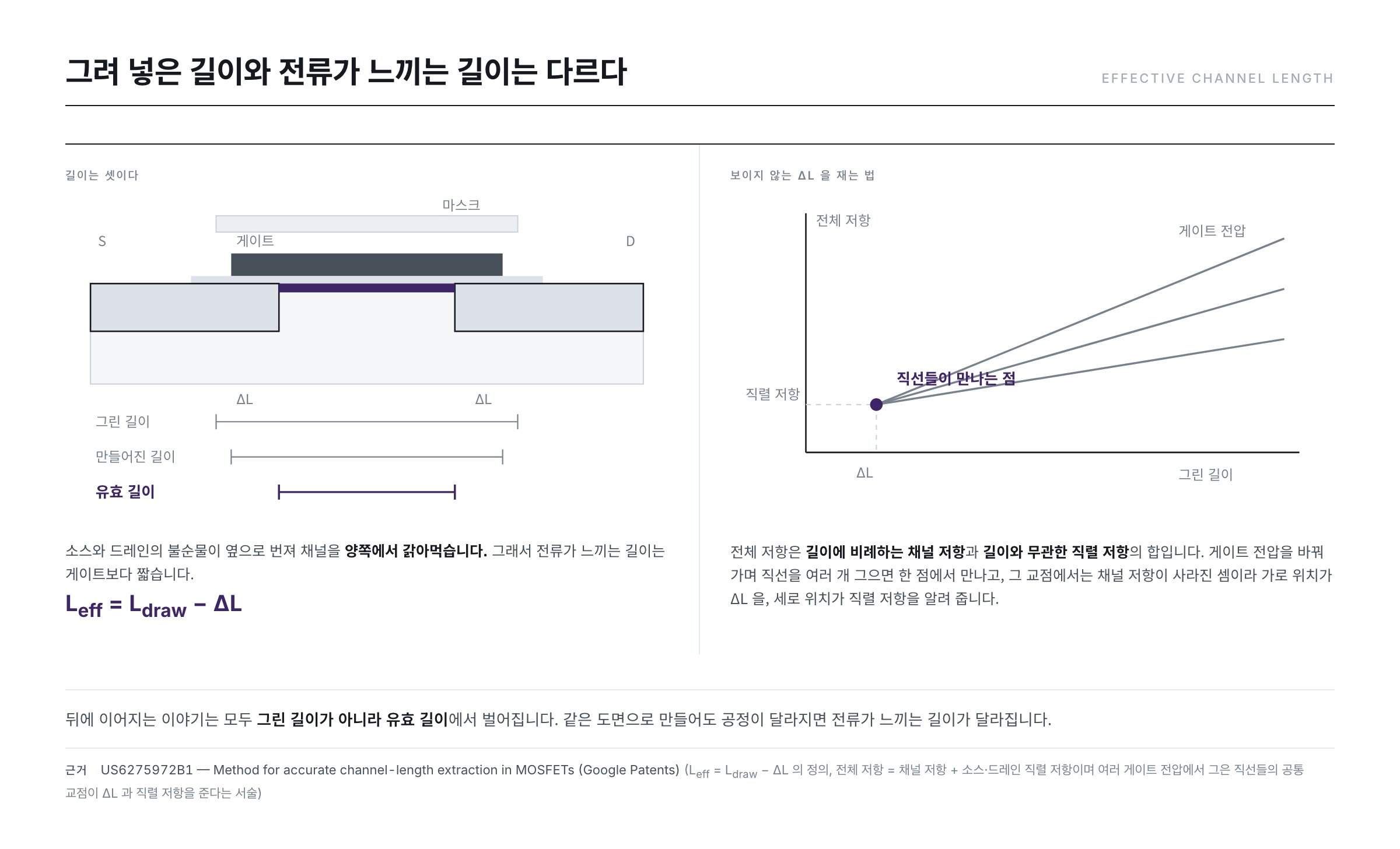
The value called "channel length" is really three values: the drawn length written on the design drawing, the fabricated length left after lithography and etching, and the effective channel length that the current feels.
The third is the shortest. The impurities of the source and drain spread out sideways and eat into the channel from both ends. The US patent US6275972B1 (a method for extracting MOSFET channel length) writes this relation as Leff = Ldraw − ΔL.
ΔL is not a value to be picked out by eye; it is measured electrically. According to the US6275972B1 specification, the total resistance is the sum of the channel resistance and the series resistance belonging to the source and drain, the former proportional to length and the latter independent of it. So one measures the total resistance of devices made with various drawn lengths, draws a straight line against drawn length, and on drawing several such lines at different gate voltages, the lines meet at a single point. At that intersection the channel resistance has in effect vanished, so the intersection reveals ΔL and the series resistance together.
The Saturation Curve Is Not Flat — Channel Length Modulation
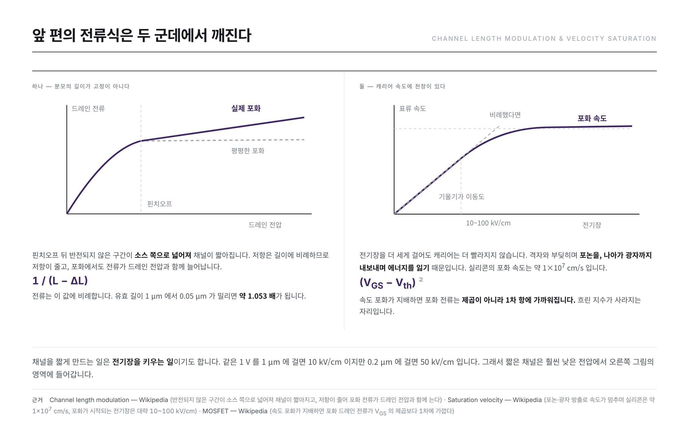
In the previous installment we said that the current in the saturation region is independent of the drain voltage. The real curve rises a little as it goes to the right.
The Wikipedia "Channel length modulation" article gives the reason. Past pinch-off, a non-inverted stretch appears between the end of the channel and the drain, and as the drain voltage rises its influence reaches further toward the source, so this stretch widens and the channel shortens. It adds that since resistance is proportional to length, a shorter channel means less resistance, so even in saturation the current grows along with the drain voltage.
How much it grows comes straight out of the previous installment's equation. The current was proportional to W/L, and the length is in the denominator. This article assumes a device of effective length 1 μm in which the pinch-off point has shifted by 0.05 μm, and calculates accordingly. The remaining channel is 0.95 μm, and the current becomes 1/0.95 = about 1.053 times, growing by a little over 5 %.
On the circuit side this slope is attached to the current equation as a (1 + λVDS) term. The "Channel length modulation" article treats λ as a value inversely proportional to the channel length, cites the fitting constant VE for a 65 nm process as about 4 V/μm, and states that if λ is 0 the output resistance is infinite. A perfectly flat saturation curve would mean a device of infinite output resistance, and there is no such device.
The "Channel length modulation" article states that this effect is more pronounced the shorter the source–drain spacing, the deeper the drain junction and the thicker the oxide. All three are conditions under which the gate holds the channel less firmly.
The Substrate Potential Pushes the Threshold Up — the Body Effect
The previous installment's equation put the source and the substrate (the body) at the same potential. The Wikipedia "Body effect" article states that in real integrated circuits the source voltage often varies dynamically while the substrate is tied to an overall reference potential. When the two part company, the threshold voltage moves.
The mechanism is the depletion layer. When the source–body junction is pushed into deeper reverse bias, the depletion layer under the gate oxide widens and more impurity ions are exposed. Since the charge the gate must balance has grown, a larger voltage is needed to form the inversion layer. The threshold rises.
Vth = Vth0 + γ ( √(2|φF| + VSB) − √(2|φF|) ), γ = √(2 εSi q NA) / Cox
This article assumes a substrate doping of 1×1017 cm−3, an oxide thickness of 10 nm, a temperature of 300 K and a source–body voltage of 1 V, and calculates accordingly. The constants used are a thermal voltage of 25.85 mV, an intrinsic carrier concentration in silicon of 9.65×109 cm−3, relative permittivities of 11.68 (silicon) and 3.9 (silicon dioxide), and a vacuum permittivity of 8.854×10⁻¹² F/m, all of them published values.
- φF = 0.02585 × ln(1×10¹⁷ ÷ 9.65×10⁹) = 0.418 V → 2φF = 0.835 V
- Cox = 3.9 × 8.854×10−12 ÷ 10 nm = 3.45×10⁻³ F/m2
- γ = √(2 × 1.034×10−10 × 1.602×10−19 × 1×1023) ÷ 3.45×10−3 = 0.527
- ΔVth = 0.527 × (√1.835 − √0.835) = about 0.23 V
The substrate is out by only 1 V, and the threshold rises by 0.23 V. Since the denominator of γ is Cox, the thinner the oxide, the smaller γ becomes. The "Body effect" article explains that a thin oxide strengthens the gate's grip and shields the channel from swings of the body. When the gate is strong, the other terminals have less say.
Shorten the Channel and the Threshold Comes Down
The body effect has nothing to do with channel length. Now comes the story in which the length itself moves the threshold. The "Short-channel effect" article seen above writes the threshold voltage of a long channel as a function of the oxide thickness and the substrate doping concentration alone; when the channel shortens, the channel length and the source and drain junction depths intrude as further variables.
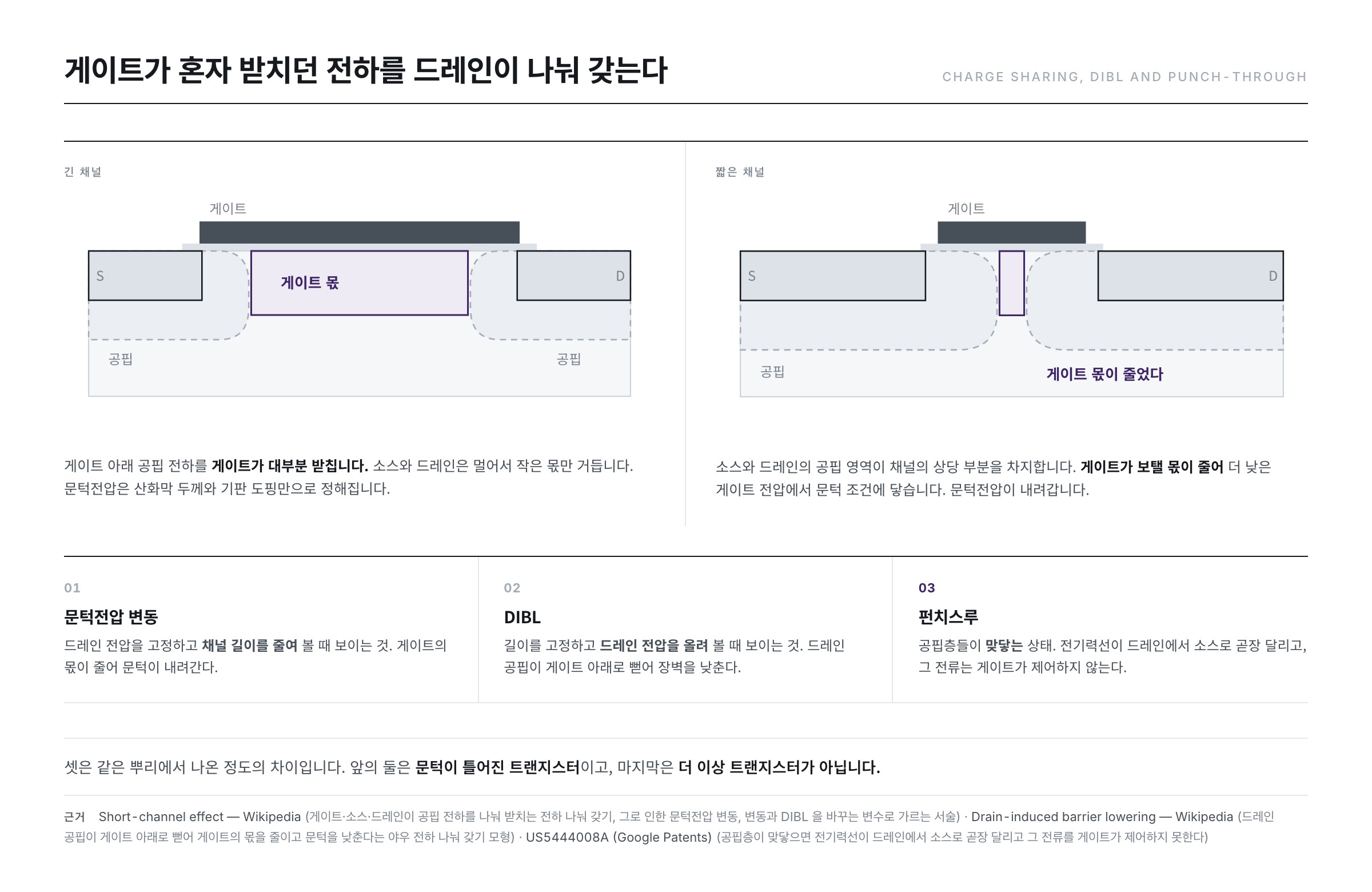
The reason is charge sharing. The depletion charge under the gate must be supported by someone. In a long channel the gate supports most of it, and the source and drain, being far away, take on only a small share. When the channel shortens, the source and drain take on a larger share.
The share the gate has to contribute then falls, so a smaller gate voltage suffices to reach the threshold condition. Since the threshold voltage is the gate voltage that reaches that condition, the threshold voltage comes down. This is threshold voltage roll-off (Vth roll-off). The "Short-channel effect" article calls it a loss of electrostatic integrity — how effectively the gate holds the channel potential.
It Breaks on the Carrier Side Too — Mobility and Velocity
So far the story has been about charge and potential. The current equation also contains how well the carriers move, and this side is no constant either.
Mobility Degradation
The channel is a thin inversion layer clinging to the interface just beneath the insulating film, and the carriers move, in effect, on a plane. The Wikipedia "Electron mobility" article sets aside surface roughness scattering as the limit on the mobility of these quasi-two-dimensional electrons, and states, on the evidence of high-resolution transmission electron microscopy, that the interface is not smooth at the atomic level and its position rises and falls by one or two atomic layers. This unevenness shakes the energy levels at the interface and causes scattering. The US patent US6548335B1 likewise points to the roughness of the interface between silicon and the oxide as the main cause of scattering.
The gate's vertical electric field creates the inversion layer by pulling it toward the interface. The higher the gate voltage, the more the carriers cling to the interface and the more often they encounter the unevenness. The Wikipedia "MOSFET" article records the consequence this way — as devices grow smaller the electric field within the channel grows stronger and the doping concentration rises, and both changes lower the carrier mobility and thus lower the transconductance.
Velocity Saturation
Mobility is the constant of proportionality in "velocity picks up in proportion to the electric field," but that proportionality does not hold forever. The Wikipedia "Saturation velocity" article states that beyond a certain high field the carriers get no faster. It is because interaction with the lattice increases, so that they give off phonons and, at still higher energies, even photons, losing energy in the process. The values the "Saturation velocity" article carries are about 1×107 cm/s for silicon, 1.2×107 cm/s for gallium arsenide and about 2×107 cm/s for 6H silicon carbide, and the field at which saturation sets in is roughly 10~100 kV/cm.
The electric field is voltage divided by distance. Put 1 V across 1 μm and that is 10 kV/cm; across 0.2 μm it is 50 kV/cm. Making the channel short is the same work as making the field strong, so a short channel enters this regime at a far lower voltage. The result changes the shape of the equation. The "MOSFET" article states that when velocity saturation dominates, the saturation drain current becomes closer to linear in VGS than quadratic. The square of the previous installment's equation disappears.
The Drain Opens the Door — DIBL and Punch-Through
DIBL (Drain-Induced Barrier Lowering) is the phenomenon in which the threshold voltage comes down as the drain voltage rises.
The Wikipedia "Drain-induced barrier lowering" article states that in a long channel the bottleneck where the channel forms is far enough from the drain to be electrostatically shielded from the drain by the substrate and the gate, and that the threshold voltage was therefore independent of the drain voltage. In a short channel the drain is close enough to touch the channel much as the gate does, so a high drain voltage can open the bottleneck and turn the transistor on ahead of time.
The mechanism is the same as in the previous section. According to the Yau charge-sharing model cited by the "Drain-induced barrier lowering" article, when the drain voltage rises the depletion region of the drain–body junction reaches in under the gate, so that the drain takes on more of the burden of balancing the depletion charge and the gate's share falls. The gate's charge then draws more carriers into the channel to keep the balance, which amounts to having lowered the threshold voltage.
It shares a root with the threshold voltage roll-off of the previous section. The "Short-channel effect" article separates the two by which variable is changed — what you see when you hold the drain voltage fixed and shorten the channel is threshold voltage roll-off; what you see when you hold the length fixed and raise the drain voltage is DIBL.
There is an order to how it progresses. The "DIBL" article states that as the channel shortens, in the subthreshold region the current curve at first shifts bodily sideways; shorten it further and the slope of the curve itself worsens, so that a larger gate voltage is needed for the same change of current; and at extreme shortness the gate fails altogether to turn the device off. Beyond a threshold merely gone astray, the very ability to turn it off collapses.
Push further and another name appears. The US patent US5444008A states that when the depletion layers touch, the lines of electric force run straight across the substrate from drain to source, and this state is called punch-through. The current that then flows is not controlled by the gate. DIBL is the gate's share shrinking; punch-through is that share effectively disappearing. The former is a transistor whose threshold has gone askew; the latter is no longer a transistor.
The Strong Field Near the Drain — Impact Ionisation and Hot Carriers
Last comes what the carriers get up to where the field has grown strong. The Wikipedia "Impact ionization" article defines impact ionisation as a process in which one energetic carrier loses energy while creating other carriers. An electron or hole with sufficient kinetic energy knocks an electron bound in the valence band up into the conduction band, and an electron–hole pair is created.
The "Impact ionization" article states the condition plainly: a sufficiently large electric field is required, and this demands a large voltage, not necessarily a large current. Where it takes place in a region of high field it can lead to avalanche breakdown. The neighbourhood of the drain is exactly that condition — the shorter the channel, the more the same voltage is dropped across a narrower stretch.
The high-energy carriers created here are called hot carriers. The Wikipedia "Hot carrier injection" article insists that "hot" refers not to the actual temperature of the device but to the effective temperature used in modelling the carrier density. The device may be cold and the carriers hot. The article states that to enter the conduction band of silicon dioxide, electrons need about 3.2 eV and holes 4.6 eV of kinetic energy.
The article says an accelerated carrier has two routes by which to lose energy.
- Colliding with an atom of the substrate and leaving behind one cooled carrier and one electron–hole pair — the impact ionisation seen above.
- Striking and breaking an Si–H bond at the interface — one interface state is created and a hydrogen atom is released into the substrate.
The interface state left by the second is the problem. The "Hot-carrier injection" article states that once interface states appear, the threshold voltage changes and the subthreshold slope worsens, with the result that the current falls and the operating frequency of the integrated circuit drops. This installment goes this far — why it happens. The story of how this accumulates to set the lifetime of a device is taken up separately in the series "Anomalies and Reliability in TFT Characteristics."
Summary
- There are three channel lengths — the drawn length, the fabricated length and the effective length the current feels. The literature writes Leff = Ldraw − ΔL, and ΔL is extracted from the intersection of the resistance lines.
- Channel length modulation — even in saturation, a rising drain voltage shortens the channel, lowering the resistance and increasing the current. A shift of 0.05 μm in 1 μm gives about 5 %.
- The body effect — when the substrate parts from the source the depletion layer widens and the threshold rises. Under the assumptions above, an offset of 1 V gives about 0.23 V.
- Threshold voltage roll-off, DIBL and punch-through — the source and drain share in supporting the depletion charge and the threshold comes down. Shorten the length and you see roll-off; raise the drain voltage and you see DIBL; go all the way and you get punch-through, which the gate does not control.
- Mobility degradation and velocity saturation — carriers are slowed by striking the roughness of the interface, and in silicon they stop at about 1×107 cm/s. The saturation current in VGS then becomes closer to linear rather than quadratic.
The names were many, but what they say is one thing. The previous installment's equation stood on the premise that the gate controls the channel by itself. Shorten the channel and the drain, the substrate, the interface, and finally the carriers' own speed limit intrude one after another. Short-channel effects are several names attached to the process by which the gate's sole dominion collapses.
Even so, the transistor still does the work of a switch. In the next installment we set switches facing each other and build the inverter, NAND and NOR — that is, logic.
References
- Short-channel effect — Wikipedia : the definition of short-channel effects, charge sharing and threshold voltage roll-off, electrostatic integrity, the distinction between roll-off and DIBL
- Channel length modulation — Wikipedia : the statement that the channel shortens so the resistance falls and the saturation current grows, the (1 + λVDS) term, infinite output resistance if λ = 0, VE ≈ 4 V/μm for a 65 nm process
- Body effect — Wikipedia : the statement that the source–body voltage widens the depletion layer and raises the threshold, the Vth equation and the definition of the coefficient γ
- Drain-induced barrier lowering — Wikipedia : why the threshold was independent of the drain voltage in a long channel, the Yau charge-sharing model, the sequence of parallel shift → slope degradation → failure to turn off
- Saturation velocity — Wikipedia : the statement that velocity stops through phonon and photon emission, the saturation velocities by material, the onset field of 10~100 kV/cm
- MOSFET — Wikipedia : the statement that under velocity saturation the saturation current is closer to linear in VGS, the statement that increasing field and doping lower the mobility
- Electron mobility — Wikipedia : the statement that surface roughness scattering limits the mobility of quasi-two-dimensional electrons, and the size of the interface unevenness
- Impact ionization — Wikipedia : the definition of impact ionisation, the statement that a large field is required but not a large current, avalanche breakdown
- Hot carrier injection — Wikipedia : the statement that "hot" refers to an effective temperature, about 3.2 eV for electrons and 4.6 eV for holes to enter silicon dioxide, the two routes of energy loss and the consequences of interface states
- US6275972B1 (Google Patents) : Leff = Ldraw − ΔL and the method of extracting ΔL from the intersection of resistance lines
- US5444008A (Google Patents) : the definition of punch-through as the depletion layers touching so that the lines of force run straight from drain to source
- US6548335B1 (Google Patents) : the statement that the main cause of carrier scattering is the roughness of the silicon/oxide interface
- Constants used in the calculations : Boltzmann constant (thermal voltage 25.85 mV) · Charge carrier density (intrinsic carriers 9.65×109 cm−3) · Relative permittivity (11.68 · 3.9) · Vacuum permittivity (8.854×10⁻¹² F/m)
- ※ The portions quoted above from Wikipedia articles are licensed under CC BY-SA 4.0.