Across eight installments we have built a single device. We put impurities into silicon to obtain P-type and N-type, joined the two to make a junction, and laid a gate on top of it to arrive at a transistor that regulates current. In the previous installment we also saw what comes along when you make it small.
And yet one transistor still computes nothing. It is only a switch that can be turned on and off. The question of this installment is a single one — join a few switches together and how does that become computation?
The answer is plain. With two switches we make "not," and with four we make "not both" and "neither." And with that four-switch part, one kind alone suffices to build every remaining piece of logic.
The operating values in this text are examples meant to show how a calculation goes, not the specifications of any particular company. Every figure quoted here was confirmed in published literature, and the sources are listed at the end.
First, the Promise to Use an Analogue Device Digitally
The transistor seen in the earlier installments is an analogue device. Raise the gate voltage a little and the current grows a little; raise it more and it grows more. Intermediate values exist in any quantity you like.
Digital circuits throw that middle away. It is settled that a voltage close to the supply reads as 1 and one close to ground reads as 0, and the stretch in between goes unused. The Wikipedia "Inverter (logic gate)" article states that digital circuits operate at fixed voltage levels corresponding to logical 0 and 1, and gives 0 V and +5 V in TTL circuits as an example.
The Wikipedia "Logic gate" article describes logic gates as made using diodes or transistors as electronic switches. A high output means drawing current from the positive supply terminal and a low output means sinking it to the negative supply terminal, the "Logic gate" article explains.
In sum, it is this. The device is analogue, but by restricting how we read it to two values we use it digitally. Why that restriction is a gain becomes clear later, when we come to noise.
The Inverter — "Not," Made from Two Switches
The simplest logic is negation. The Wikipedia "Inverter (logic gate)" article defines the NOT gate as the gate implementing logical negation, and states that it outputs a bit of the opposite value to the input bit. The truth table has only two lines — a 0 in gives a 1, a 1 in gives a 0.
When One Side Opens, the Other Closes
There are several ways to build it. The "Inverter (logic gate)" article first introduces the approach of attaching a resistor to a single NMOS and points out its weakness — because current keeps flowing through the resistor in one of the two states, it is at a disadvantage in power and in processing speed.
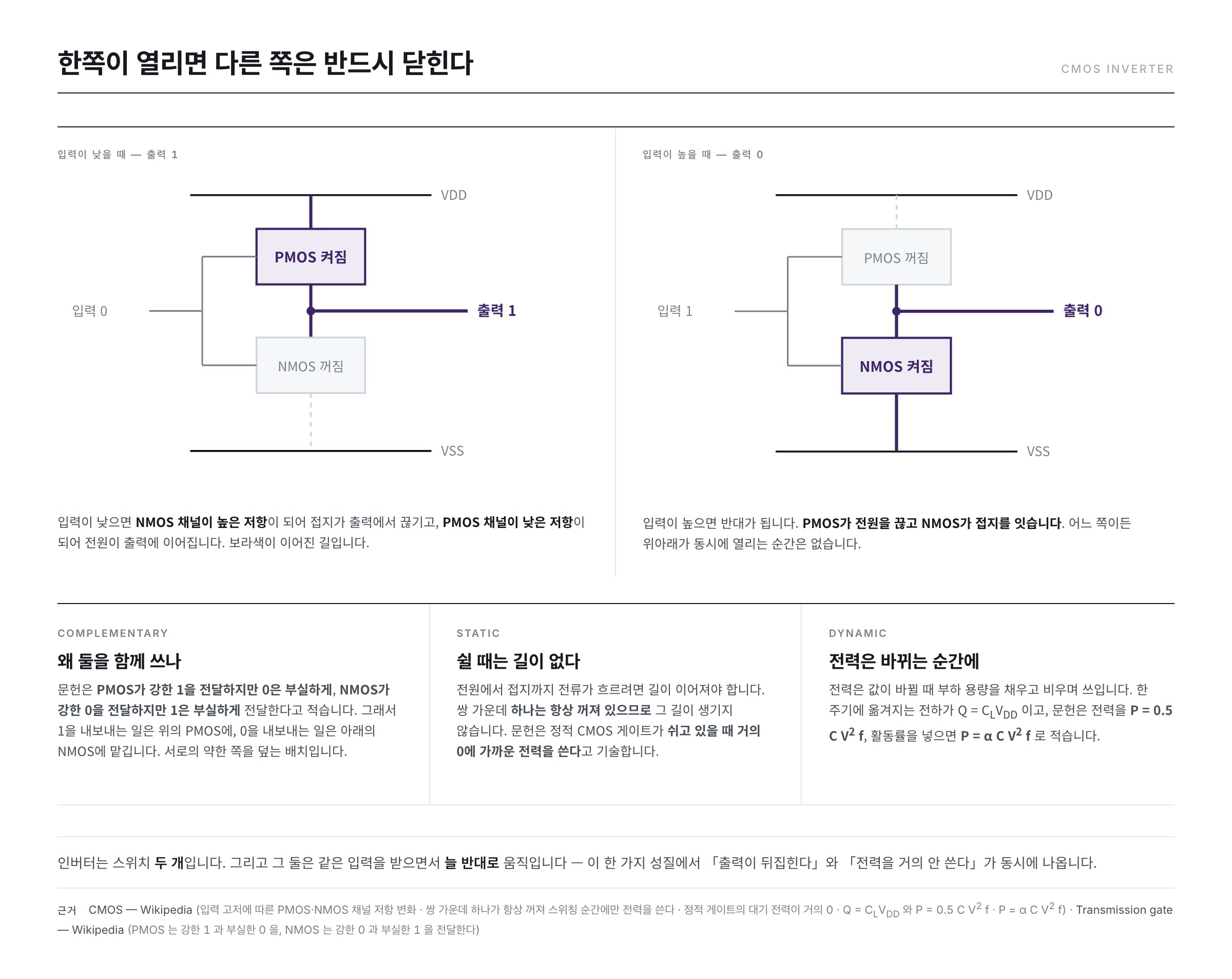
The alternative is CMOS. A PMOS is put where the resistor was. The wiring described by the Wikipedia "CMOS" article is this. A PMOS goes on top, an NMOS below, and both gates are connected together to the same input. The top touches the supply Vdd, the bottom touches ground Vss, and the point where the two meet is the output.
The operation as recorded by the "CMOS" article takes two lines.
- When the input is low — the channel of the NMOS goes into a high-resistance state, cutting ground off from the output, and the channel of the PMOS goes into a low-resistance state, connecting the supply to the output. The output is 1.
- When the input is high — the reverse. The PMOS goes into a high-resistance state and cuts off the supply, and the NMOS goes into a low-resistance state and connects ground. The output is 0.
They receive the same input and respond in exactly opposite ways. The name "complementary" comes from this. The Wikipedia "Inverter (logic gate)" article states that this arrangement greatly reduces power consumption because in both logic states one of the transistors is always off.
Why the PMOS on Top and the NMOS Below, of All Things
One may ask whether the order could be swapped. It cannot. It is because the value each of the two devices passes well is different.
The Wikipedia "Transmission gate" article states this property in one sentence — the PMOS passes a strong 1 but passes 0 poorly, while the NMOS passes a strong 0 but passes 1 poorly.
So the arrangement is settled. The job of putting out a 1 goes to the PMOS, which passes 1 well, and the job of putting out a 0 goes to the NMOS, which passes 0 well. That is why the PMOS is on top and the NMOS below. Each device covers the other's weak side.
And So It Uses Almost No Power
For current to flow from supply to ground, a path must be continuous. In a CMOS inverter one of the two, top or bottom, is always broken, so that path does not exist. The Wikipedia "CMOS" article puts it this way — since one of the pair of MOSFETs is always off, this series combination draws significant power only in the moment of passing between on and off.
The "CMOS" article describes a static CMOS gate as consuming power close to 0 while at rest. NMOS logic, by contrast, keeps a path from Vdd to Vss always open while the transistor is on, and so keeps spending power.
Power Is Spent at the Moment the Value Changes
Where, then, is power spent? What we saw in the fourth installment returns here. Wherever there is a junction, a capacitor comes along whether you want it or not.
The Wikipedia "CMOS" article states that a CMOS circuit consumes power each time it switches, as it charges various load capacitances. It adds that gate capacitance and wiring capacitance make up most of it, with drain and source capacitances also present. In one complete cycle, current flows from VDD into the load capacitance and charges it, and on discharge it flows out of the charged capacitance to ground.
The "CMOS" article writes the charge moved in one cycle as Q = CLVDD, and multiplies this by the switching frequency and the average voltage to obtain the power.
P = 0.5 C V2 f
Since most gates do not change value on every clock, the "CMOS" article attaches an activity factor α and rewrites it as P = α C V2 f.
What this equation says is clear. Power is proportional to the number of times the value changed. Sit still and almost none is spent. And the voltage enters squared — lowering the supply voltage is the most powerful means of reducing power.
But "almost 0" is not "0." The "CMOS" article states that in modern devices, whose threshold voltage has been lowered for speed, subthreshold leakage current has become significant, and that even designs containing many circuits that are not actively switching spend power through this leakage. The short-channel problem seen in the previous installment reappears here under the heading of power.
The Transfer Characteristic — the Steeper the Middle, the Better
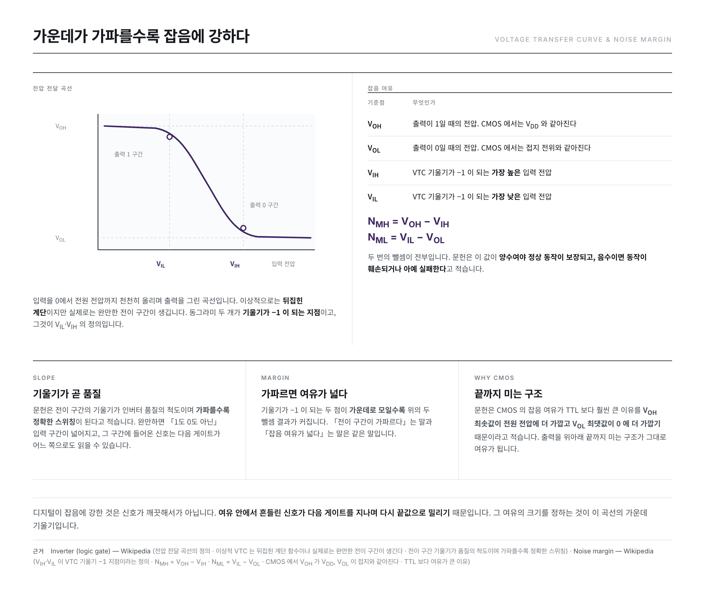
The quality of an inverter is measured with a single picture. It is the curve of output voltage drawn while the input voltage is raised slowly from 0 to the supply voltage. The Wikipedia "Inverter (logic gate)" article calls this the voltage transfer curve (VTC) and states that from it one can obtain the noise tolerance, the gain and the operating logic levels.
The "Inverter (logic gate)" article describes the ideal VTC as an inverted step function. It is a shape in which the output drops vertically at one point. In a real device a gradual transition region appears. And it adds — the slope of this transition region is a measure of quality, and the steeper it is the more accurate the switching.
Why Is the Slope Quality?
When the slope is gradual, the input range that is "neither 1 nor 0" grows wider. A signal falling in that range can be read either way by the next gate. That is where the computation goes wrong.
What fixes this allowance as a number is the noise margin. The Wikipedia "Noise margin" article defines it as the maximum noise amplitude that can be added to the worst-case noise-free input level without taking the output outside the permitted logic levels.
There are four reference points.
- VOH — the voltage when the output is 1. The "Noise margin" article states that in a CMOS inverter this value becomes equal to VDD.
- VOL — the voltage when the output is 0. In CMOS it becomes equal to the ground potential.
- VIH — defined as the highest input voltage at which the slope of the VTC is −1.
- VIL — the lowest input voltage at which the slope is −1.
The margins are two subtractions.
NMH = VOH − VIH and NML = VIL − VOL
The "Noise margin" article states that these values must be positive for correct operation to be guaranteed, and that if they are negative operation is impaired or fails outright.
Here the shape of the curve and the margin connect. The closer the two points of slope −1, VIH and VIL, gather toward the middle, the larger the results of the two subtractions. To say the transition region is steep is to say the noise margin is wide.
The "Noise margin" article also gives the reason CMOS has a far larger noise margin than TTL — because the minimum of VOH is closer to the supply voltage and the maximum of VOL is closer to 0. The CMOS structure, which pushes the output all the way to the top and bottom rails, becomes the margin itself. It is in the same vein that the "CMOS" article names high noise immunity and low static power consumption as the two important characteristics of this technology.
The earlier promise to "throw away the middle" pays here. In analogue, noise remains as error just as it is. Use only two values, and a signal that has wobbled within the margin is pushed back to the end values as it passes the next gate, and is gone.
Two Ways to Join Switches — NAND and NOR
Take the inverter and raise the inputs to two. There are only two ways to do it — join them in series or join them in parallel.
Series says "both must be on for it to conduct"; parallel says "only one need be on." Those two sentences are exactly logical AND and logical OR. Since in CMOS the top and bottom must be opposite, putting the bottom in series makes the top parallel of itself.
NAND — the Bottom in Series
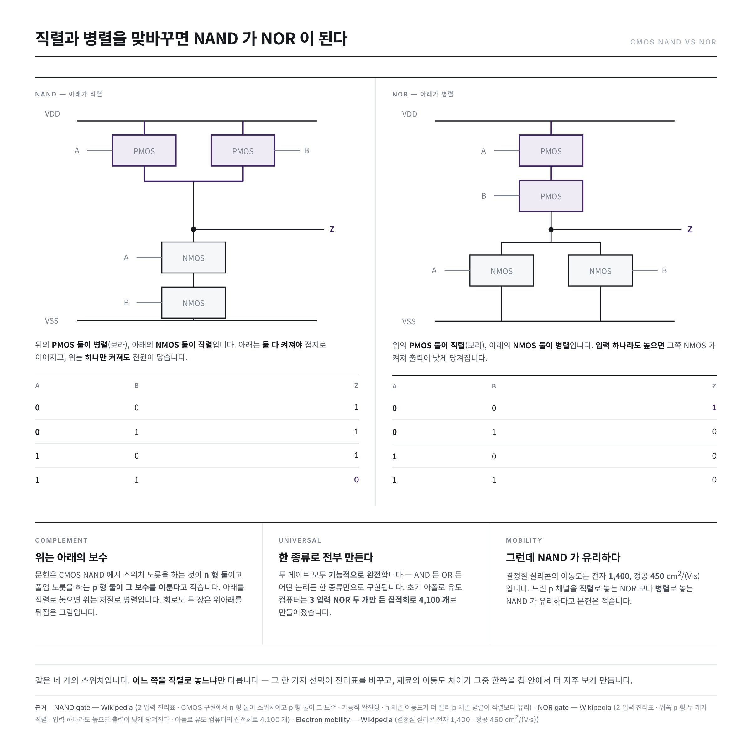
The Wikipedia "NAND gate" article describes the CMOS implementation this way. Playing the part of switches are two n-type transistors, and playing the part of the pull-up resistor are two p-type transistors, this p-type pair forming the complement of the n-type pair.
The word complement settles the arrangement. If the two NMOS below are in series, the two PMOS above are in parallel. Let us follow the four inputs.
- A=0, B=0 — both NMOS below are off, so there is no path to ground. Both PMOS above are on, so the supply reaches the output. Output 1.
- A=0, B=1 — only one NMOS below is on. Being in series, the path is still broken. Above is parallel, so the supply reaches the output even with only one side on. Output 1.
- A=1, B=0 — the mirror image of the line above. Output 1.
- A=1, B=1 — both NMOS below are on and the series path is continuous. Both PMOS above are off. Output 0.
It is 0 only when both are 1. This matches the 2-input truth table carried by the Wikipedia "NAND gate" article, and the "NAND gate" article states that this function is logically the same as NOT(A AND B).
NOR — the Bottom in Parallel
Put it the other way round and you get the opposite gate. The Wikipedia "NOR gate" article describes the CMOS implementation as one in which the function of the pull-up resistor is taken by a series connection of the two upper p-type transistors. Below is its complement, two parallel NMOS.
The "NOR gate" article sums up the operation this way — if any one of the inputs is high, the corresponding n-channel device turns on and the output is pulled low; otherwise the output is pulled up.
- A=0, B=0 — both below are off, so there is no path to ground, and both of the series PMOS above are on, so the supply reaches the output. Output 1.
- A=0, B=1 — below is parallel, so even one being on connects to ground. Above is series, so even one being off breaks it. Output 0.
- A=1, B=0 — the mirror image of the line above. Output 0.
- A=1, B=1 — both paths below are continuous and above is completely broken. Output 0.
It is 1 only when both are 0. The "NOR gate" article defines NOR as the gate that gives a high output only when both inputs are low.
Set the two circuit diagrams side by side and they are the same picture turned upside down. Series and parallel have merely exchanged places.
Either One Would Do, and That One Is NAND
Building Everything from One Kind
The Wikipedia "NAND gate" article states that NAND possesses functional completeness. It means that AND, OR, or any other logic function whatever can be implemented with NAND alone, and NOR has the same property. The "NAND gate" article adds that an entire processor can be built from NAND gates alone.
The "Logic gate" article even records the history of this fact. Charles Sanders Peirce showed, in 1880~1881, that the functions of all other logic gates could be reproduced with NOR gates alone, or with NAND gates alone. This is why the two are called universal logic gates.
Machines have actually been built that way. The "NOR gate" article states that the early Apollo Guidance Computer was built from 4,100 integrated circuits each containing only two 3-input NOR gates. The calculator that went to the Moon was one kind of gate.
But in CMOS the NAND Side Has the Advantage
If both are universal gates, it would seem either would do. And yet they part. The reason already appeared in the seventh installment — holes are slower than electrons.
The table in the Wikipedia "Electron mobility" article records the mobilities in crystalline silicon as 1,400 for electrons and 450 cm2/(V·s) for holes. That is a difference of more than threefold. The "Electron mobility" article describes hole mobility as generally lower.
Lower mobility means that at the same size it cannot deliver the same current. A PMOS must be wider to match an NMOS, and widening it increases the gate capacitance. Capacitance, as seen in the earlier section, becomes delay and power directly. On top of that, devices joined in series add resistance. Putting an already slow PMOS in series, two at a time, is therefore the disadvantageous choice.
The Wikipedia "NAND gate" and "NOR gate" articles record this in the same sentence — in CMOS the NAND gate is more efficient than the NOR gate, because the charge mobility of the n-channel MOSFET is faster than that of the p-channel, so that the parallel connection of the two p-channel devices realised in NAND is more favourable than the series connection in NOR. Both articles therefore close with the same sentence, that NAND is preferred over NOR in CMOS circuits.
One property of a material has pushed all the way through to the choice of circuit. Holes are slow → the PMOS must be widened → series PMOS is to be avoided → NAND is what you see more often inside a chip.
Summary
- Digital is not a property of the device but a promise. It is a decision to read the voltage of an analogue device as only two values.
- The CMOS inverter stacks a PMOS and an NMOS one above the other and ties the gates together. The literature states that in both logic states one of them is always off. The top is the one that passes 1 well, the bottom the one that passes 0 well.
- In the static state there is no path joining supply and ground, so it spends power close to 0 while at rest. Power is spent filling and emptying capacitance when the value changes, following P = α C V2 f.
- The steep middle of the voltage transfer curve is the quality. The two points of slope −1 are VIH and VIL, and the noise margins are given by NMH = VOH − VIH and NML = VIL − VOL.
- Put the bottom in series and it is NAND; in parallel and it is NOR. Both are functionally complete, so one kind alone builds all of logic. But holes are slow and series PMOS is unfavourable, so NAND is preferred in CMOS circuits.
Here the series closes. Looking back, it joins into a single line. We set out from the fact that the resistance of a material lies between that of a metal and that of an insulator, put in impurities to make P-type and N-type, joined the two to obtain a junction that flows one way only, saw the capacitor that comes along with it, and raised the terminals to three to reach a transistor that regulates the flow. We decided to read it as on and off only, joined four of them together, and out came logic. It is the road from a stone to computation.
In the next series, "TFT Characteristic Parameters," the numbers that measure how well this transistor has been made — threshold voltage, mobility, on/off ratio, subthreshold swing — are taken apart one by one.
References
- CMOS — Wikipedia : the inverter wiring and the channel resistances for high and low inputs, the statement that one of the pair is always off so power is spent only in the moment of switching, standby power close to 0, P = 0.5 C V2 f · P = α C V2 f, subthreshold leakage
- Inverter (logic gate) — Wikipedia : the definition and truth table of the NOT gate, the weakness of the resistive-load approach, the statement that one transistor is always off in both logic states, fixed logic voltage levels (TTL 0 V · +5 V), the voltage transfer curve and the statement that the slope of the transition region is a measure of quality
- Noise margin — Wikipedia : the definition of the noise margin, the definition of VIH and VIL as the points of VTC slope −1, the NMH and NML equations, the statement that in CMOS VOH equals VDD and VOL equals ground, and the reason the margin is larger than in TTL
- Transmission gate — Wikipedia : the statement that the PMOS passes a strong 1 and a poor 0 while the NMOS passes a strong 0 and a poor 1
- NAND gate — Wikipedia : the 2-input truth table and the equivalence with NOT(A AND B), the CMOS implementation in which two n-type devices are the switches and two p-type devices their complement, functional completeness, the reason NAND is more efficient than NOR
- NOR gate — Wikipedia : the 2-input definition and truth table, the CMOS implementation in which the two upper p-type devices are in series, the explanation that the output is pulled low if any one input is high, the 4,100 integrated circuits of the Apollo Guidance Computer
- Logic gate — Wikipedia : the statement that diodes and transistors are used as electronic switches, the meaning of high and low outputs, the account that Peirce showed in 1880~1881 that all gates could be reproduced with NOR alone or NAND alone
- Electron mobility — Wikipedia : the electron mobility 1,400 and hole mobility 450 cm2/(V·s) in crystalline silicon
- ※ The portions quoted above from Wikipedia articles are licensed under CC BY-SA 4.0.