Turn on a smartphone and a picture appears on the screen. That picture is made of millions of tiny fragments of light, each lit at its own assigned brightness. But to tell each fragment "you shall be this bright," every fragment needs a switch of its own attached to it.
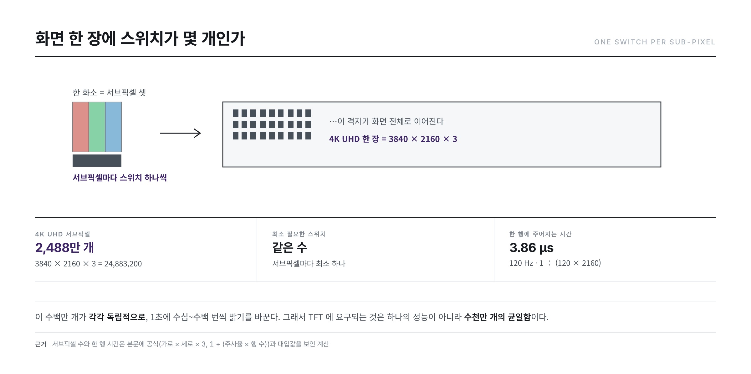
That switch is the thin-film transistor (TFT). A single 4K UHD screen (3840×2160) has 3840 × 2160 × 3 = 24.88 million subpixels, and it needs at least that many switches.
This series is about that switch. What it is, by what principle it turns on and off, and why its material has been torn up and replaced three times over the past 60 years.
The condition values that appear in the calculations in this text (dimensions, voltages, capacitances and so on) are examples chosen to show how the calculation is done, and the device structures and material compositions are likewise the generic forms described in the open literature — they are not the device specifications or drawings of any particular company. Everything is treated only at the level anyone can verify in published papers, patents and encyclopedias, and the sources are listed at the end of each part.
Take the name apart and half is already explained
The name "thin-film transistor" has two parts.
- Transistor — a component that controls the flow of electricity with an electrical signal. It is a switch and a valve at the same time.
- Thin film — it means the component was built as a separately deposited thin layer.
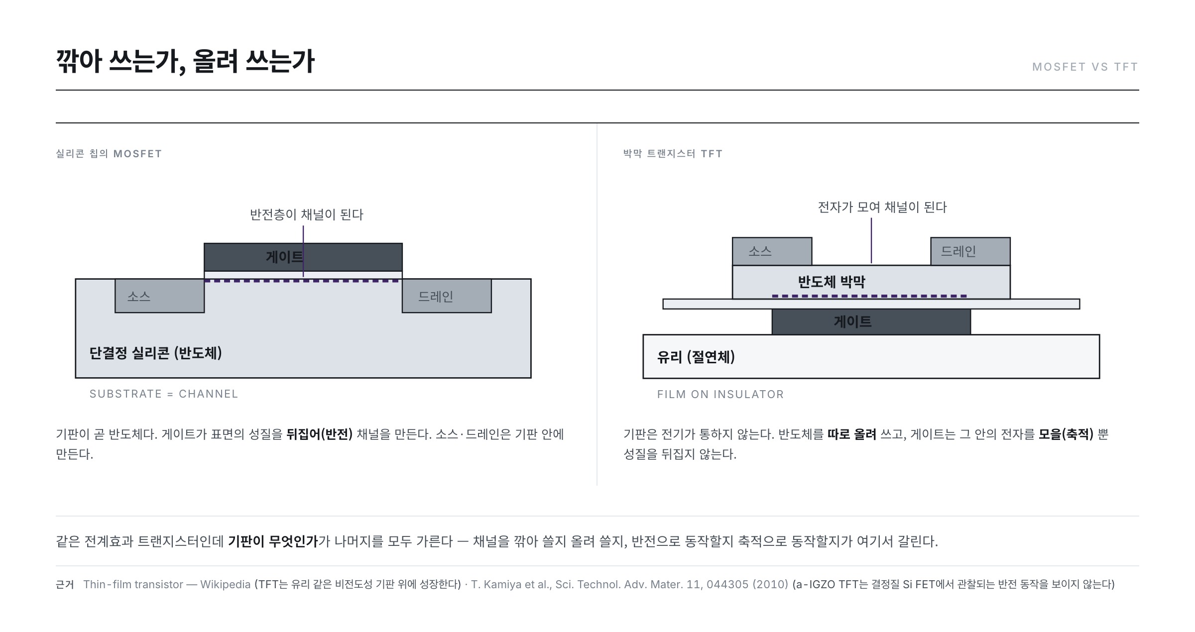
The second part is the key. The transistors inside a computer chip are made by carving a block of single-crystal silicon. The material is already there, and it is sculpted. A TFT is the opposite. The substrate is glass, which does not conduct electricity, and the materials the transistor needs are coated on top of it one layer at a time. The Wikipedia article "Thin-film transistor" likewise describes a TFT as being grown "on a supporting (but non-conducting) substrate, such as glass."
This one difference gives rise to every other difference.
What a transistor does — a faucet
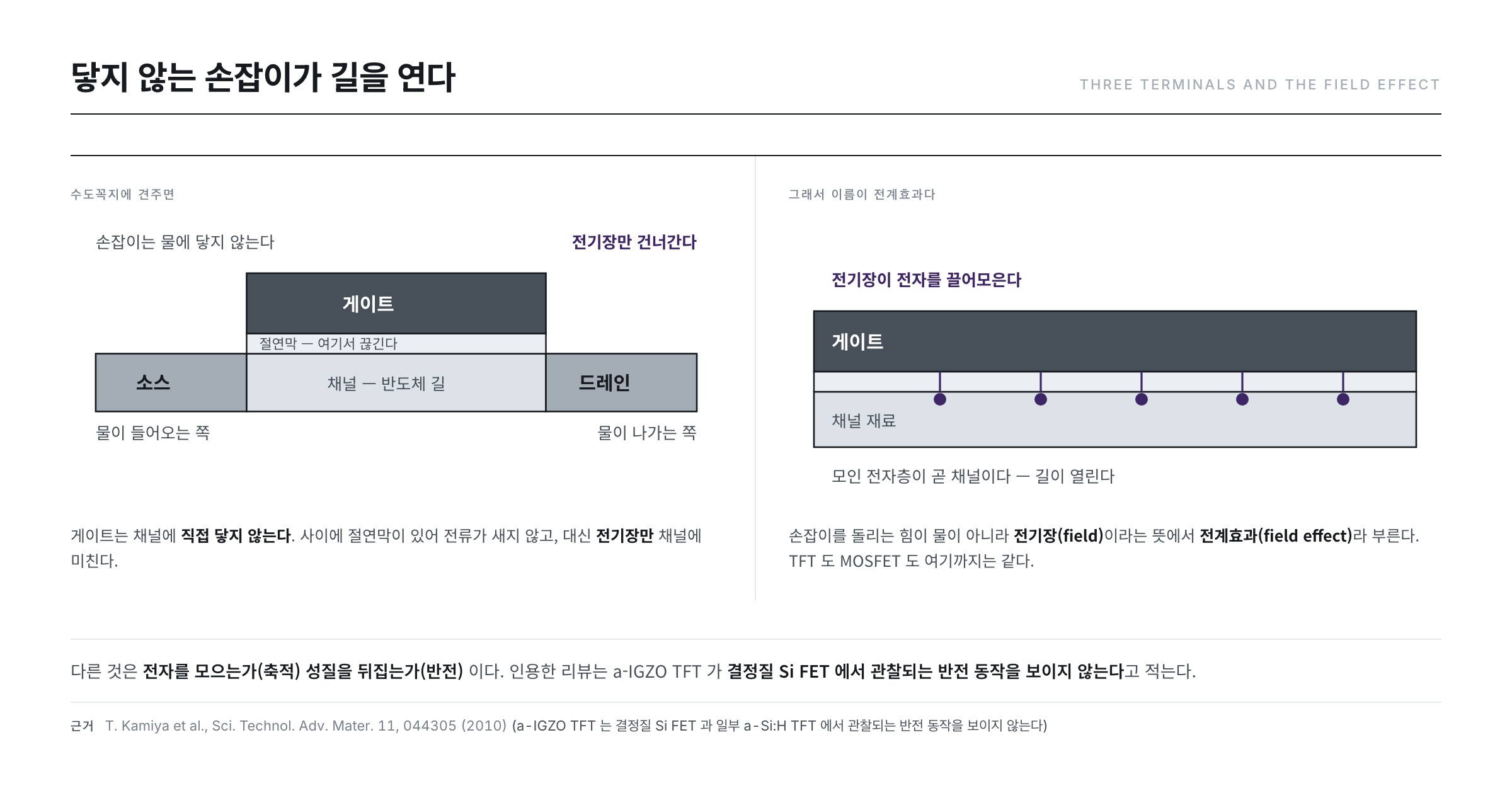
A transistor has three terminals. In the analogy of water they are as follows.
- Source — where the water comes in
- Drain — where the water goes out
- Gate — the faucet handle
Between the source and the drain lies a semiconductor path called the channel. The gate does not touch this path directly — a thin insulating film sits in between. So even when a voltage is applied to the gate, no current leaks into the gate; instead, only an electric field reaches the channel. That field gathers or scatters the electrons in the channel, opening and closing the path.
Because the force that turns the handle is not water but an electric field, this scheme is called the field effect. Both the TFT and the MOSFET in a computer chip are field-effect transistors. Up to this point they are the same.
So what is different
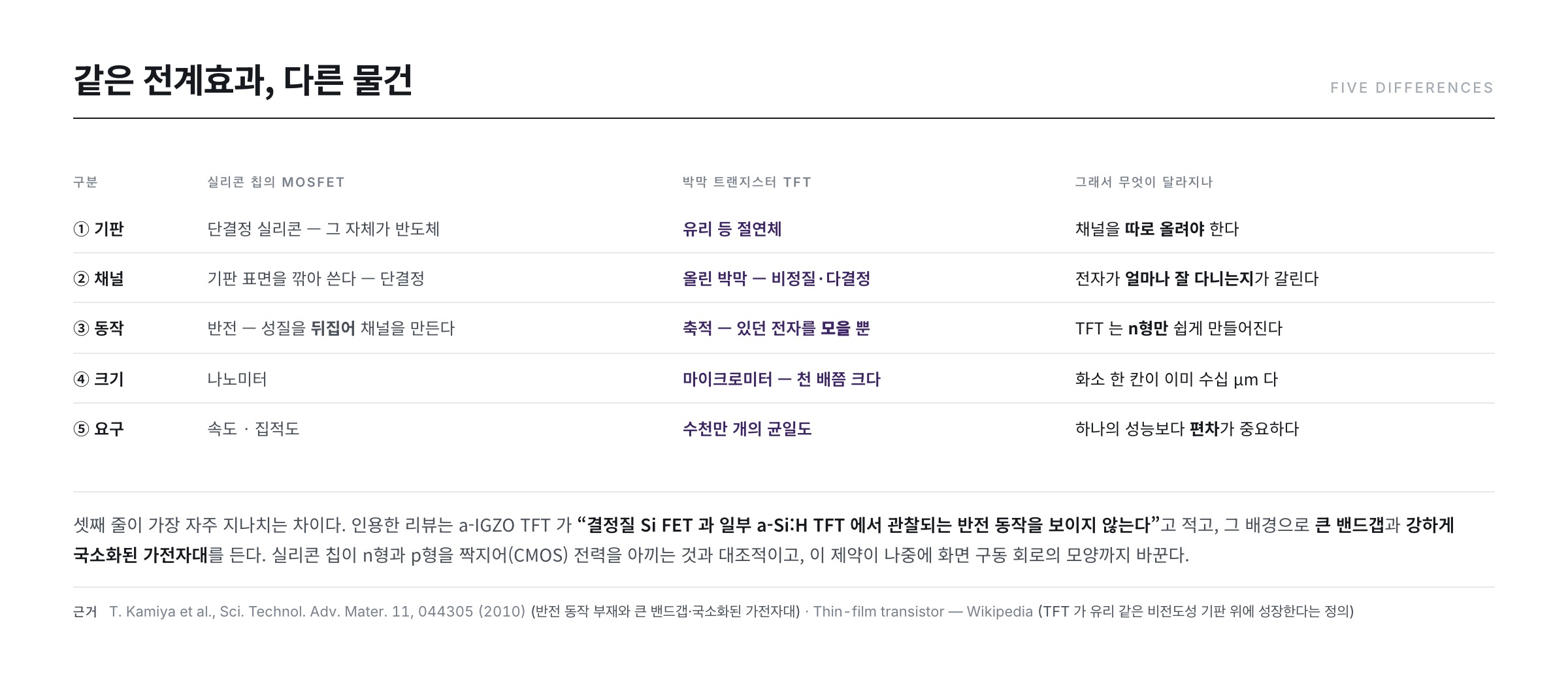
Even though both rely on the field effect, a TFT and the transistor in a silicon chip are quite different objects. The differences fall into five strands.
① Substrate — semiconductor or insulator
In a MOSFET, the single-crystal silicon wafer is itself the semiconductor. The transistor's channel is the surface of that wafer. A TFT's substrate is glass, which does not conduct, so the semiconductor to be used as the channel has to be laid on separately.
② Channel — carved out or laid on
When carved out, the channel is the single crystal itself, with its atoms lined up in regular order. When laid on, it is either amorphous, with a disordered atomic arrangement, or polycrystalline, a collection of small crystal grains. This difference decides how well electrons travel, and that is the subject of Part 2 of this series.
③ Mode of operation — inversion or accumulation
This is the difference most often passed over.
A silicon MOSFET operates by inversion. The silicon at the channel site is originally p-type, rich in holes (positive carriers), but when a positive voltage on the gate draws electrons to the surface, that thin layer alone flips its character and becomes n-type. That flipped layer is the channel.
A TFT operates by accumulation. The channel material is n-type from the start, with electrons as its carriers, and the gate voltage merely gathers those electrons near the insulator. It collects what was already there without flipping anything.
The review that Kamiya, Nomura and Hosono published in Sci. Technol. Adv. Mater. in 2010 states this explicitly — it writes that "a-IGZO TFTs do not show the inversion operation observed in crystalline Si FETs and some a-Si:H TFTs," and gives as the reasons the oxide's large band gap and strongly localized valence band. Since holes cannot be used, there is nothing to flip.
One practical consequence follows. TFTs are easy to make only as n-type, using electrons; p-type, using holes, is difficult. This contrasts with silicon chips, which pair n-type and p-type (CMOS) to save power. This constraint will later reshape even the form of the circuits that drive the screen.
④ Size — nanometers or micrometers
The transistors in the latest semiconductor chips are on the nanometer (one billionth of a meter) scale. TFTs are on the micrometer (one millionth of a meter) scale, about a thousand times larger. There is no need to make them small — the spot a TFT occupies is a single pixel visible to the human eye, and that pixel is itself tens of micrometers across.
⑤ What is demanded — speed or uniformity
A chip's transistors must be fast. TFTs must be identical to one another, tens of millions of times over. On a screen, if one transistor passes just a little more current than its neighbors, that pixel looks brighter, and the human eye picks up the difference as a blotch. The spread across tens of millions matters more than the performance of any single transistor.
Powell's paper on a-Si TFT physics in IEEE Trans. Electron Devices in 1989 makes this point at its end — it reports that the uniformity of large-area transistor arrays for displays is excellent, with a threshold-voltage spread of 0.5–1.0 V.
| Item | MOSFET on a silicon chip | Thin-film transistor (TFT) |
|---|---|---|
| Substrate | Single-crystal silicon (semiconductor) | Insulator such as glass |
| Channel | The substrate surface as is | Separately deposited thin film (amorphous / polycrystalline) |
| Operation | Inversion | Accumulation |
| Polarity | n-type and p-type used in pairs (CMOS) | Mostly n-type |
| Typical dimension | Nanometers | Micrometers |
| What matters most | Speed, integration density | Uniformity across tens of millions |
Why on glass at all — let us calculate the area
The question "if the performance is worse, why insist on glass" comes naturally. The answer lies in area, and two multiplications are enough to confirm it.
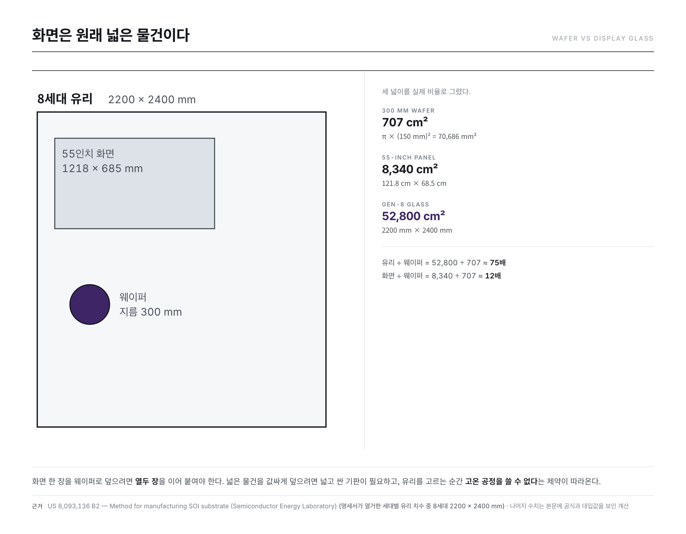
The representative wafer in a semiconductor fab is a 300 mm diameter disc. The area of a circle is π × radius², so
π × (150 mm)² = 3.14159 × 22,500 mm² = 70,686 mm² ≈ 707 cm²
Display glass substrates, on the other hand, are sized by generation. The specification of Semiconductor Energy Laboratory's US patent US 8,093,136 B2 lists the dimensions by generation, and among them Generation 8 is 2200 mm × 2400 mm. It is a rectangle, so simply multiplying gives
2200 mm × 2400 mm = 5,280,000 mm² = 52,800 cm²
Dividing the two values,
52,800 cm² ÷ 707 cm² ≈ 75
One sheet of glass corresponds to about 75 300 mm wafers.
The same holds when we look at a single screen. To find the area of a 55-inch 16:9 screen: the 55-inch diagonal is 55 × 2.54 = 139.7 cm, and width : height : diagonal = 16 : 9 : √(16²+9²) = 16 : 9 : 18.36, so
width = 139.7 × 16 ÷ 18.36 ≈ 121.8 cm · height = 139.7 × 9 ÷ 18.36 ≈ 68.5 cm
area = 121.8 × 68.5 ≈ 8,340 cm²
With 300 mm wafers you would have to stitch together 8,340 ÷ 707 ≈ 12 of them just to barely cover one screen. A screen is a wide object by nature, and covering a wide object cheaply requires a wide and cheap substrate. Glass meets that condition.
And the moment glass is chosen, a price follows. Glass softens at high temperature, so the 1,000 ℃-class processes used to make single-crystal silicon cannot be used. Only semiconductors that can be made at low temperature remain candidates, and that constraint has driven the history of TFT materials for the past 60 years.
Three upheavals
1962 — The first transistor made by deposition alone
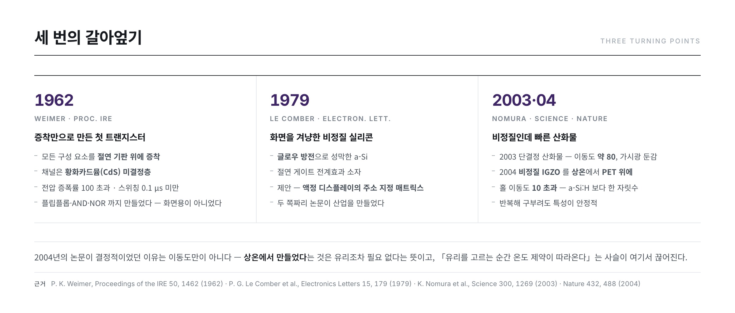
Paul K. Weimer of RCA published "The TFT — A New Thin-Film Transistor" in Proceedings of the IRE in 1962. The paper introduces it as a transistor made by depositing all of its components onto an insulating substrate, and describes the operating principle as controlling "majority carriers injected into a wide-band-gap semiconductor by means of an insulated control gate." The channel material was a microcrystalline layer of cadmium sulfide (CdS).
The reported performance was a voltage gain above 100, a transconductance above 10,000 μmho, and a switching time below 0.1 μs. The paper states that flip-flops, AND gates and NOR gates were built with this device. From the start it was aimed at computer components, not at displays.
For reference, the Wikipedia article "Thin-film transistor" records that earlier still, in February 1957, John Wallmark of RCA filed a patent for a thin-film MOSFET.
1979 — Amorphous silicon aimed at the screen
Le Comber, Spear and Ghaith of the University of Dundee published "Amorphous-silicon field-effect device and possible application" in Electronics Letters in 1979. They built an insulated-gate field-effect device from amorphous silicon (a-Si) deposited by glow discharge, and wrote the proposal corresponding to the "possible application" in the title thus — that this device could be used to advantage in the addressing matrix of a liquid-crystal display panel.
The screens we use today start from this two-page paper.
2003 · 2004 — An oxide that is amorphous yet fast
Amorphous silicon was cheap and could be coated over a wide area, but its electrons were slow. According to the values compiled in the 2010 review by Kamiya et al. cited above, the saturation mobility of a-Si:H TFTs lies in the range 0.24–0.60 cm²V⁻¹s⁻¹.
Hosono's group opened a different path. In Science in 2003, Nomura et al. reported a transparent transistor with single-crystal InGaO₃(ZnO)₅ as the channel and amorphous hafnium oxide as the gate insulator — a field-effect mobility of about 80 cm²V⁻¹s⁻¹, an on/off current ratio of about 10⁶, and operation insensitive to visible light.
The Nature paper the following year, 2004, was decisive. Nomura et al. deposited amorphous In-Ga-Zn-O (a-IGZO) on PET film at room temperature, and reported that the Hall mobility exceeded 10 cm²V⁻¹s⁻¹, an order of magnitude larger than hydrogenated amorphous silicon. The saturation mobility of the transparent TFTs fabricated on the PET sheet was 6–9 cm²V⁻¹s⁻¹, and the characteristics were stable even when the sheet was bent repeatedly.
The received wisdom that amorphous means slow breaks here. Why it breaks is the subject of Parts 9 and 10 of this series.
One number called mobility
The number that runs through all three transitions is mobility. It expresses how readily electrons are pulled along when an electric field is applied, and its unit is cm²V⁻¹s⁻¹. Placing the values from the 2010 review by Kamiya et al. cited above side by side gives the following.
| Channel material | Saturation mobility (cm²V⁻¹s⁻¹) | Source |
|---|---|---|
| Hydrogenated amorphous silicon (a-Si:H) | 0.24 ~ 0.60 | Kamiya 2010 |
| Amorphous oxide (a-IGZO) | 8.2 ~ 12.6 | Kamiya 2010 |
The same review summarizes that a-IGZO TFTs have a field-effect mobility 10 times larger and a defect density 10 times smaller than a-Si:H TFTs, and also cites reported examples of up to 18 cm²V⁻¹s⁻¹, and up to 35.8 cm²V⁻¹s⁻¹ in an etch-stopper structure.
Why this number matters becomes clear from a simple calculation. When drawing a 4K screen at 120 Hz, the time given to one row is
1 ÷ (120 Hz × 2160 rows) = 3.86 μs
. If we assume a storage capacitance of 0.5 pF per pixel and a required voltage swing of 5 V (both are example values to show the calculation), the required charging current is
I = C × ΔV ÷ t = 0.5 pF × 5 V ÷ 3.86 μs ≈ 0.65 μA
This current has to be passed by a single micrometer-scale transistor — and by all 24.88 million of them almost identically. If the material's electrons are slow, charging does not finish in time, and that pixel comes out darker than intended. That is why mobility is the number that limits a screen's size, resolution and refresh rate all at once.
Where this series is going
"The Transistor That Draws the Screen" covers the device itself in fourteen parts.
- Part 1 (01–05) Device basics — the principle of the field effect and the four structures, how to read the characteristic curves, setting up the current equation, how to measure the threshold voltage
- Part 2 (06–11) Three channels — what amorphous silicon, low-temperature polycrystalline silicon and oxide each gained and each lost
- Part 3 (12–14) Devices age — why the threshold voltage drifts, the problems light causes, and how to measure them
The next installment covers how the gate actually forms the channel, and the four device structures that diverge according to the order in which gate, channel and electrodes are stacked.
References
- P. K. Weimer, "The TFT — A New Thin-Film Transistor," Proceedings of the IRE 50, 1462 (1962) : the first TFT made by deposition alone on an insulating substrate — channel material (CdS), majority-carrier control by an insulated gate, voltage gain, transconductance and switching time
- P. G. Le Comber, W. E. Spear, A. Ghaith, "Amorphous-silicon field-effect device and possible application," Electronics Letters 15, 179 (1979) : glow-discharge amorphous-silicon field-effect device and the proposed application to the addressing matrix of liquid-crystal displays
- K. Nomura et al., "Thin-Film Transistor Fabricated in Single-Crystalline Transparent Oxide Semiconductor," Science 300, 1269 (2003) : single-crystal InGaO₃(ZnO)₅ channel with HfO₂ insulator, mobility about 80 cm²V⁻¹s⁻¹, on/off ratio about 10⁶, insensitivity to visible light
- K. Nomura et al., "Room-temperature fabrication of transparent flexible thin-film transistors using amorphous oxide semiconductors," Nature 432, 488 (2004) : room-temperature deposition of a-IGZO on PET, Hall mobility above 10 (an order of magnitude over a-Si:H), TTFT saturation mobility 6–9 on PET, stable characteristics under repeated bending
- T. Kamiya, K. Nomura, H. Hosono, "Present status of amorphous In–Ga–Zn–O thin-film transistors," Sci. Technol. Adv. Mater. 11, 044305 (2010) : basis for accumulation operation (absence of inversion), saturation mobility values for a-Si:H and a-IGZO, the tenfold comparison of mobility and defect density, reported maximum mobilities
- M. J. Powell, "The physics of amorphous-silicon thin-film transistors," IEEE Trans. Electron Devices 36, 2753 (1989) : uniformity of large-area TFT arrays and threshold-voltage spread of 0.5–1.0 V
- US 8,093,136 B2 — Method for manufacturing SOI substrate (Semiconductor Energy Laboratory) : glass-substrate dimensions by generation listed in the specification — basis for the Generation 8 size of 2200 mm × 2400 mm in the text
- Thin-film transistor — Wikipedia : the definition of a TFT as grown on an insulating substrate such as glass, and the historical record of Wallmark's 1957 patent filing and Weimer's 1962 development
- ※ Portions of the list above quoted from the Wikipedia article are subject to the CC BY-SA 4.0 license.