In the previous part we compared a transistor to a water tap. But the handle of this tap never touches the water. Between the gate and the channel sits an insulating film that carries no current, and the gate reaches across it with an electric field only.
How can it open a path without touching anything? This part covers that principle. It then looks at the four device structures that diverge according to the order in which gate, channel and electrodes are stacked.
The condition values that appear in the calculations (thickness, voltage, permittivity and so on) are examples chosen to show how the calculation works, and the device structures are likewise the general forms described in the public literature.
The gate is one plate of a capacitor
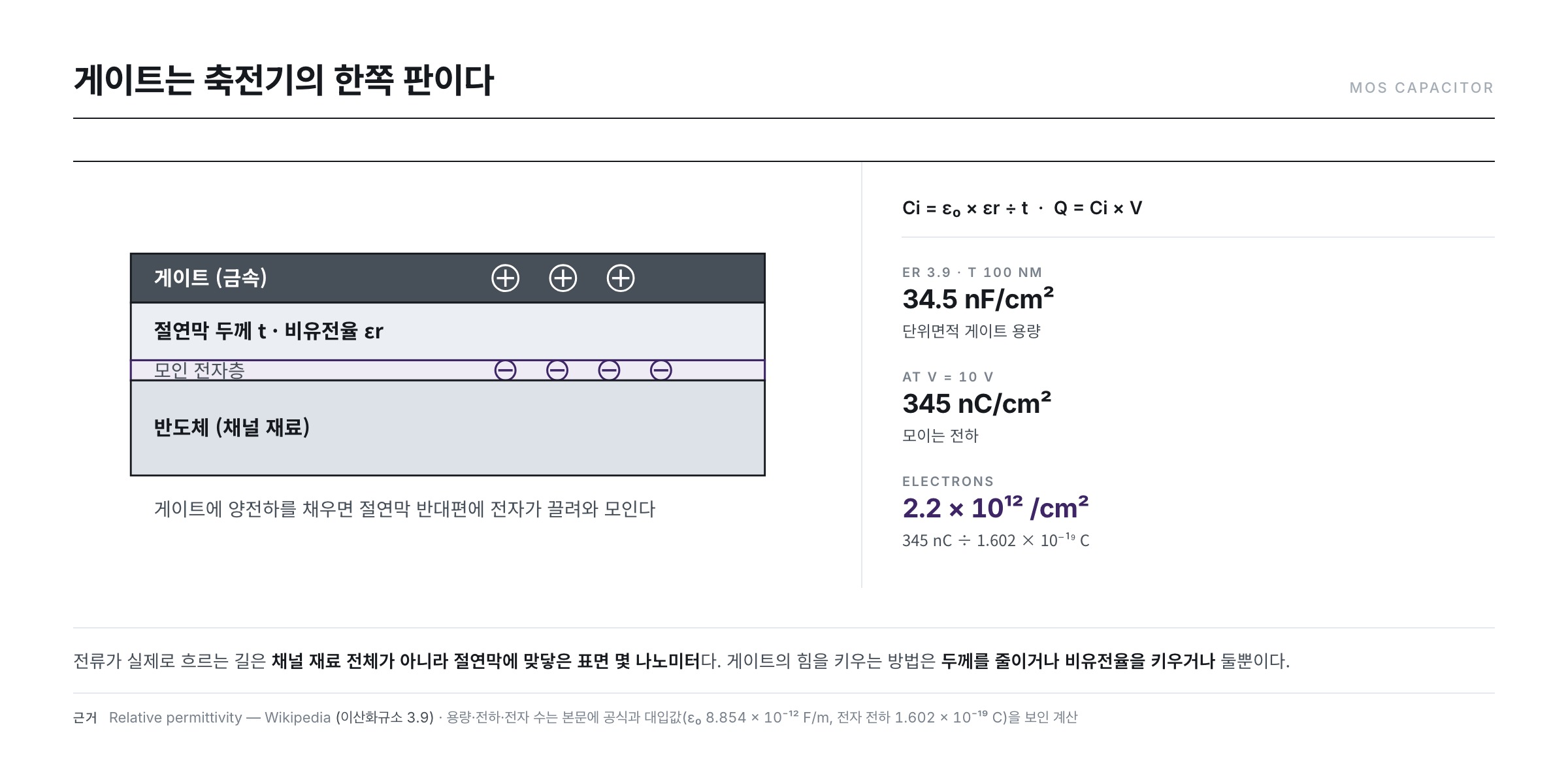
Look at the stack of gate, insulator and semiconductor from the side, and what you see is a capacitor. Because Metal, Oxide and Semiconductor are stacked in that order, it is called the MOS structure.
The behaviour of a capacitor comes down to one thing — push charge onto one plate, and an equal amount of opposite charge gathers on the other plate. Apply a positive voltage to the gate to fill it with positive charge, and electrons are drawn in and accumulate at the semiconductor surface on the far side of the insulator. Those accumulated electrons are the channel.
How many gather can be calculated. The capacitance per 1 cm² of area, that is, the gate capacitance per unit area, is
Ci = ε₀ × εr ÷ t
Here ε₀ is the permittivity of vacuum, 8.854 × 10⁻¹² F/m, εr is the relative permittivity of the insulator, and t is the insulator thickness. Suppose an insulator with relative permittivity 3.9 is laid down 100 nm thick (example values chosen to show the calculation):
Ci = 3.9 × 8.854 × 10⁻¹² F/m ÷ (100 × 10⁻⁹ m) = 3.45 × 10⁻⁴ F/m²
Since 1 m² is 10⁴ cm², converting to cm² gives 3.45 × 10⁻⁸ F/cm², or about 34.5 nF/cm².
Apply a voltage to this and the charge that gathers is Q = Ci × V. Suppose the gate voltage is 10 V above the threshold voltage:
Q = 34.5 nF/cm² × 10 V = 345 nC/cm² = 3.45 × 10⁻⁷ C/cm²
The charge of a single electron is 1.602 × 10⁻¹⁹ C, so dividing gives the number of electrons gathered per 1 cm² of area.
3.45 × 10⁻⁷ ÷ 1.602 × 10⁻¹⁹ ≈ 2.2 × 10¹² per cm²
That means 2 trillion electrons spread as a thin layer directly beneath the insulator in every square centimetre. This layer is only nanometres thick, so the path through which current actually flows in the transistor is not the whole channel material but only the few nanometres of surface touching the insulator.
Why there is a threshold voltage
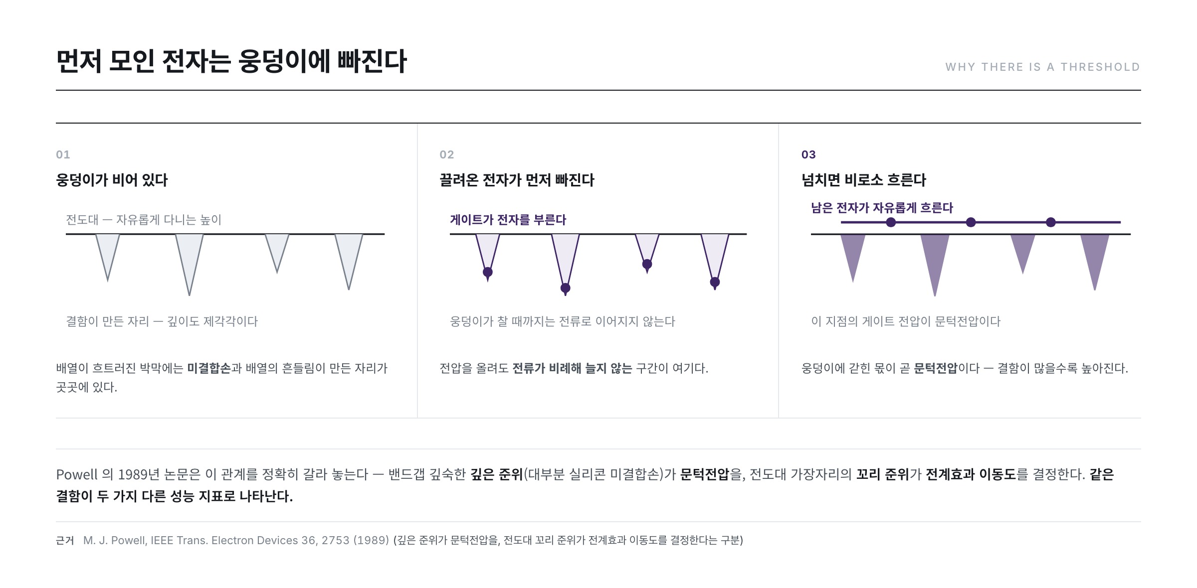
Raising the gate voltage gradually from 0 does not make the current grow in proportion right away. Only beyond a certain voltage does current begin to flow properly, and that voltage is called the threshold voltage (Vth).
The reason is that the first electrons to gather get trapped. A thin-film semiconductor has a disordered atomic arrangement, so it is full of sites created by bonds left unpaired (dangling bonds) or by fluctuations in the arrangement. These sites are energetic hollows, and the electrons drawn in fall into them first. Until the hollows are reasonably full, no matter how many electrons are summoned, none of them turn into current.
Powell's 1989 paper on a-Si TFT physics in IEEE Trans. Electron Devices draws this relationship precisely — the deep states lying far inside the band gap (mostly silicon dangling bonds) determine the threshold voltage, while the tail states trailing off the conduction band edge determine the field-effect mobility.
Deep and numerous hollows raise the threshold voltage; a long tail at the edge keeps catching electrons and slows them down. This means that the same defects show up as two different performance metrics, and it is a viewpoint we will keep returning to when comparing materials in the second half of this series.
Thinner insulator, or higher permittivity
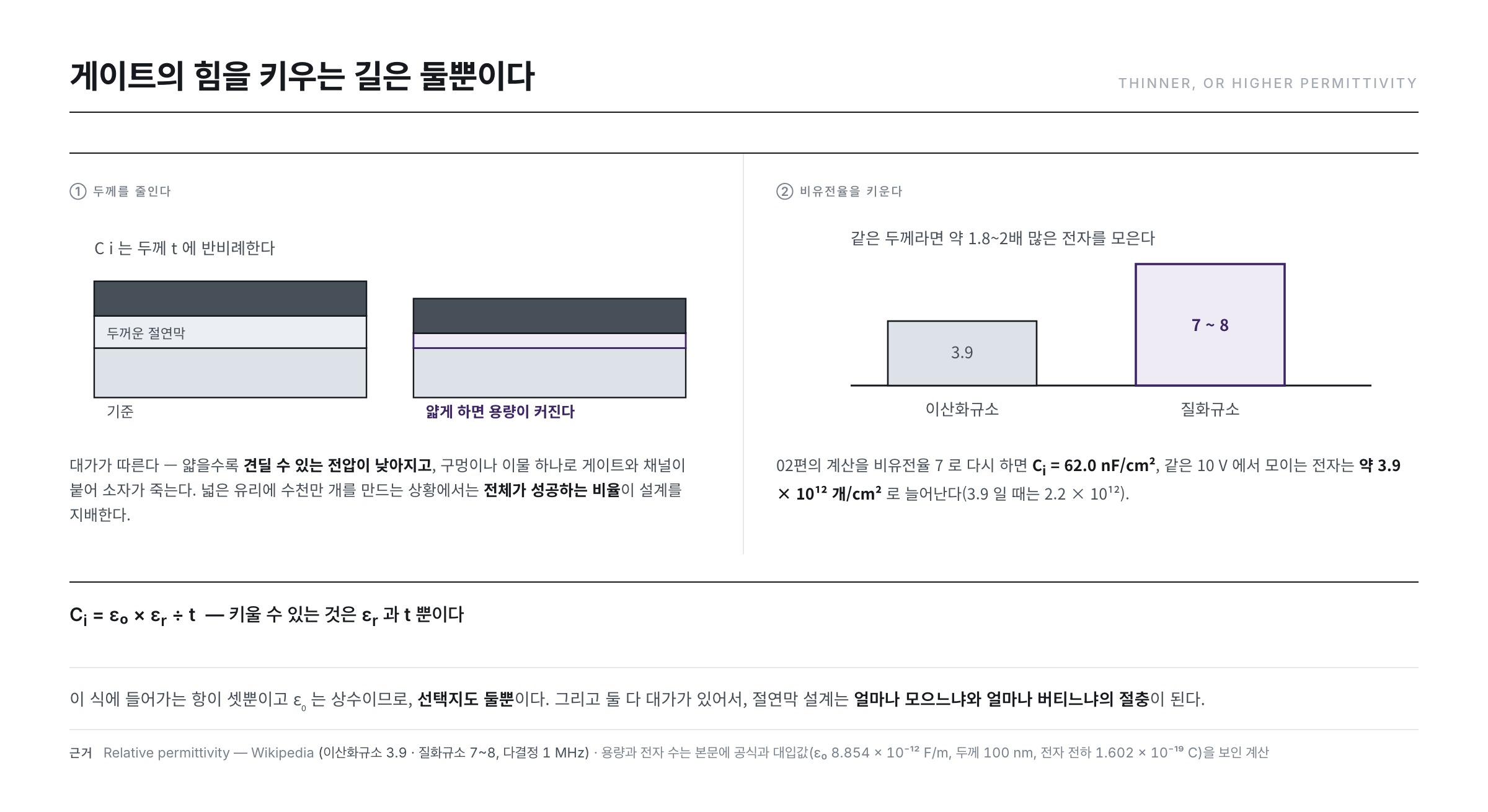
Look again at the earlier equation Ci = ε₀εr/t and you can see there are only two ways to strengthen the gate: reduce the thickness t, or raise the relative permittivity εr.
According to the values in the Wikipedia article "Relative permittivity", the relative permittivity of silicon dioxide is 3.9, and that of silicon nitride is 7–8 (polycrystalline, 1 MHz). At the same thickness, silicon nitride gathers roughly 1.8–2 times as many electrons as silicon oxide at the same voltage. Redoing the earlier calculation with a relative permittivity of 7 gives
Ci = 7 × 8.854 × 10⁻¹² ÷ (100 × 10⁻⁹) = 6.20 × 10⁻⁴ F/m² = 62.0 nF/cm²
so that the electrons gathered at the same 10 V increase to about 3.9 × 10¹² per cm².
Reducing the thickness works on the same principle, but it comes at a price. The thinner the insulator, the lower the voltage it can withstand, and a single pinhole or particle in a thin film shorts the gate directly to the channel and kills the device. When tens of millions of devices are being made on one large sheet of glass, the fraction that succeeds as a whole, rather than the performance of any one, dominates the design.
Four structures — a question of stacking order
A TFT is built by stacking layers. That naturally raises two questions.
- Lay the gate down before the channel, or cover it over afterwards — bottom-gate vs top-gate
- Attach the source and drain electrodes to which side of the channel — below the channel (bottom-contact) vs above it (top-contact)
The combinations of the two questions give four cases. The 2010 review by Kamiya, Nomura and Hosono takes these combinations as the axes for classifying device structures, and uses two names alongside them.
- Coplanar — a structure in which the source and drain lie in the same plane as the channel layer. Seen from the gate, the electrodes and the channel are on the same side.
- Staggered — a structure in which the source/drain and the gate lie on opposite sides of the channel. The name means the layers are offset.
Add whether the gate is on top or at the bottom and the four names are complete — top-gate coplanar, top-gate staggered, bottom-gate coplanar, and bottom-gate staggered. The Wikipedia article "Thin-film transistor" also shows these four branches with a "cross-section of four common thin-film transistor structures".
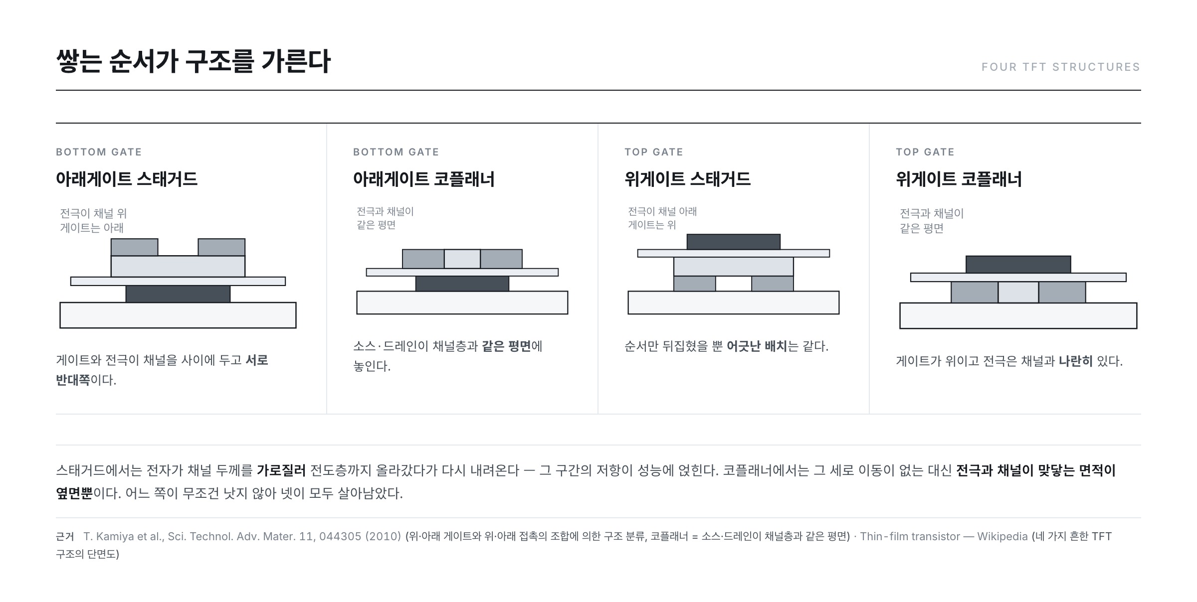
What changes with the structure becomes visible when you follow the path the current actually travels.
In the staggered structure, electrons leaving the source climb across the channel thickness up to the conducting layer near the insulator, flow sideways, and then cross the thickness again to exit at the drain. Because the electrons cross up and down twice, the resistance of those segments is added to the overall performance.
In the coplanar structure, the electrodes and the conducting layer are in the same plane, so there is no such vertical travel. Instead, the electrode and channel touch only along the side face, which makes the contact area hard to enlarge.
Neither is unconditionally better. The favourable structure differs by material and by the process used with it, and that is why all four have survived.
Two ways to protect the channel
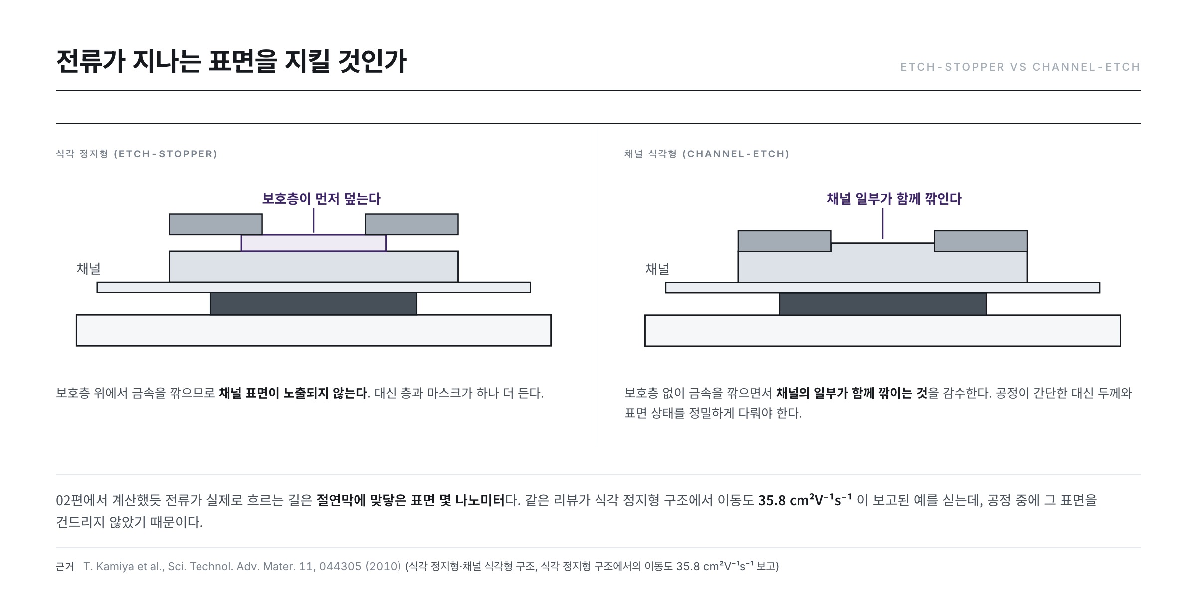
The bottom-gate staggered structure hides one process problem. The channel is laid down, the source and drain metal is deposited on top of it, and then the two electrodes must be separated. But in the course of etching away the metal, the channel surface directly beneath is damaged as well. And the path the current flows through is precisely those few nanometres of surface.
The 2010 review by Kamiya et al. cited above treats two structures for this side by side.
- Etch-stopper — a protective layer is deposited over the channel first, and the metal is etched on top of it. The channel is never directly exposed, so its surface is preserved. The cost is one more layer and one more mask.
- Channel-etch — the metal is etched without a protective layer, accepting that part of the channel is etched away along with it. The process is simpler, but channel thickness and surface condition must be controlled precisely.
The same review reports an example of a mobility of 35.8 cm²V⁻¹s⁻¹ in an etch-stopper bottom-gate staggered structure, and the explanation above makes clear why this structure yields such a high value — the surface the current travels through was never touched during processing.
In summary
- The gate is one plate of a capacitor, and the channel is the layer of electrons gathered on the opposite side.
- The number of electrons gathered is calculated from Ci = ε₀εr/t and Q = CiV.
- The first electrons to gather are trapped at defect sites, and that share is the threshold voltage.
- Structures branch four ways as top/bottom gate × coplanar/staggered, and the shape of the current path differs.
- The channel surface is easily damaged during processing, which is why the etch-stopper and channel-etch types diverged.
The next part covers how to read a device made this way — how the threshold voltage, subthreshold slope, mobility and on/off ratio are extracted from a single transfer-characteristic curve.
References
- T. Kamiya, K. Nomura, H. Hosono, "Present status of amorphous In–Ga–Zn–O thin-film transistors," Sci. Technol. Adv. Mater. 11, 044305 (2010) : structure classification by combinations of top/bottom gate and top/bottom contact, definition of the coplanar structure (source and drain in the same plane as the channel layer), etch-stopper and channel-etch structures, reported mobility of 35.8 cm²V⁻¹s⁻¹ in the etch-stopper structure
- M. J. Powell, "The physics of amorphous-silicon thin-film transistors," IEEE Trans. Electron Devices 36, 2753 (1989) : the distinction that deep states (silicon dangling bonds) determine the threshold voltage and conduction-band tail states determine the field-effect mobility
- Relative permittivity — Wikipedia : silicon dioxide 3.9, silicon nitride 7–8 (polycrystalline, 1 MHz) — basis for the relative permittivities in the gate capacitance calculation
- Thin-film transistor — Wikipedia : cross-sections of the four common TFT structures
- ※ Portions of the list above quoted from Wikipedia articles are subject to the CC BY-SA 4.0 licence.