Suppose you have a transistor in your hands. How do you tell whether it is a good device or a bad one?
The answer is a single curve. Sweep the gate voltage slowly while recording the current that flows, and a curve is drawn; from that one curve come four numbers that describe the character of the device. This part is about how to read that curve.
The condition values that appear in the calculations below are examples, chosen to show how the calculation is done.
The transfer curve — turning the handle and measuring the water
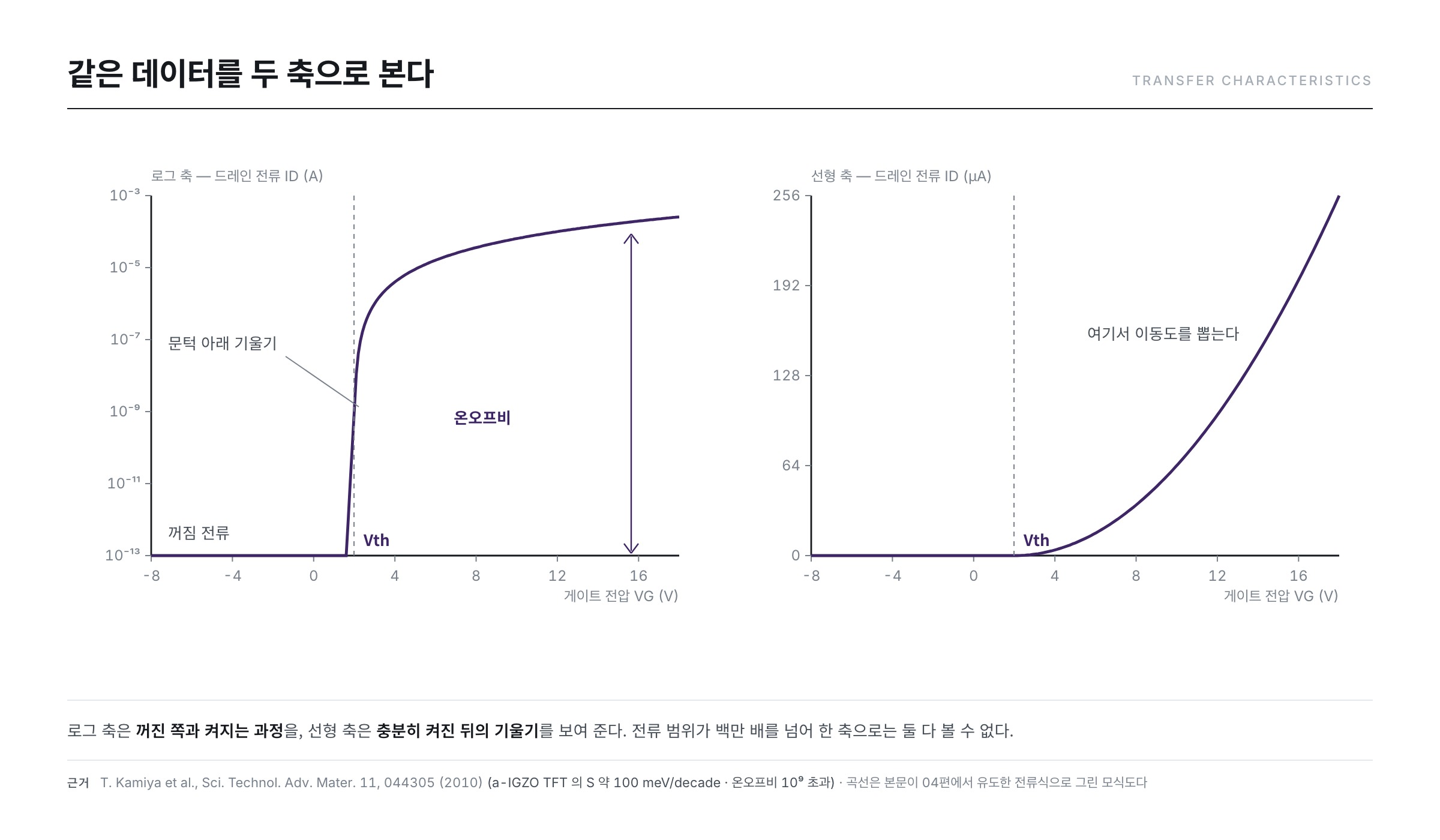
The measurement is simple. Hold the drain at a fixed voltage and change only the gate voltage (VG) slowly while recording the drain current (ID). It is like turning a tap handle little by little and measuring how much water comes out. The VG–ID curve obtained this way is called the transfer curve.
This curve, however, is drawn with the vertical axis on a logarithmic scale. The reason is that the range of the current is absurdly wide. The current in the off state is at the picoampere level (10⁻¹² A) and in the on state at the microampere level (10⁻⁶ A), a difference of more than a million times. Drawn on a linear scale, the off side appears as a straight line glued to the floor, and no information can be read from it.
So in practice the same data is drawn on a log axis and a linear axis, overlaid. The log axis shows the off side and the process of turning on; the linear axis shows the slope after the device is fully on. Each axis yields a different number.
The first number — threshold voltage
Threshold voltage (Vth) is the gate voltage at which the device "begins to turn on in earnest". As we saw in the previous part, the first electrons gathered are trapped in defect sites, and current flows properly only after that puddle has filled to some extent.
The threshold voltage matters because circuits are designed on the assumption of that value. Every pixel on the screen receives the same gate voltage, so if the threshold voltage differs from device to device, different currents flow at the same voltage, and that difference shows up as brightness mura.
There is a trap in this number, though — its value depends on how it is measured. The curve has no point labelled "on from here". This problem alone is treated separately in Part 05.
The second number — subthreshold swing
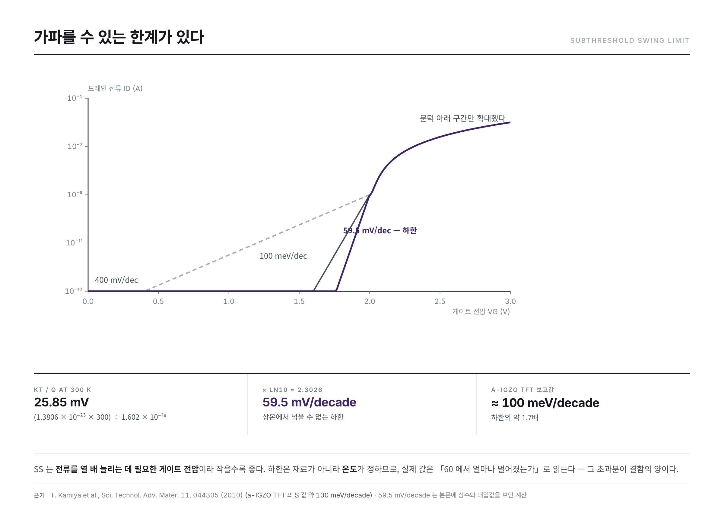
On the curve there is a steep section connecting the off state and the on state, that is, the part below the threshold voltage. The value expressing how steep this section is is the subthreshold swing (SS).
The definition is inverted — it is not a slope but the gate voltage needed to increase the current tenfold.
SS = ΔVG ÷ Δ(log₁₀ ID) [unit: V/decade]
The smaller the value, the better. It means the current rises sharply with only a small increase in voltage, so the switch turns on and off crisply.
There is a theoretical lower limit — let us calculate it ourselves
This value has a lower limit that no device, however good, can cross. The probability of an electron crossing the energy barrier is determined exponentially by temperature, and as a result the lower limit at room temperature is calculated as (kT/q) × ln10.
Let us put in the constants. Boltzmann's constant k = 1.3806 × 10⁻²³ J/K, absolute temperature T = 300 K, and the electron charge q = 1.602 × 10⁻¹⁹ C.
kT/q = (1.3806 × 10⁻²³ × 300) ÷ 1.602 × 10⁻¹⁹ = 4.142 × 10⁻²¹ ÷ 1.602 × 10⁻¹⁹ ≈ 0.02585 V
Multiplying by ln10 = 2.3026, the factor that links the natural logarithm to the common logarithm, gives
SSmin = 0.02585 V × 2.3026 ≈ 0.0595 V/decade = about 59.5 mV/decade
This means that at room temperature no field-effect transistor can be steeper than about 60 mV/decade. This value is set by temperature, independent of material or design. So when looking at the SS of a real device, one asks "how far has it moved away from 60" — and that excess tells how many defects there are.
As an example of a real value, the 2010 review by Kamiya, Nomura and Hosono gives an S value of about 100 meV/decade for a-IGZO TFTs. That is approaching within roughly 1.7 times the theoretical lower limit.
The third number — mobility
Mobility (μ) expresses how readily electrons are dragged along when an electric field is applied, and its unit is cm²V⁻¹s⁻¹. As we saw in Part 01, this value limits the resolution and refresh rate of the screen.
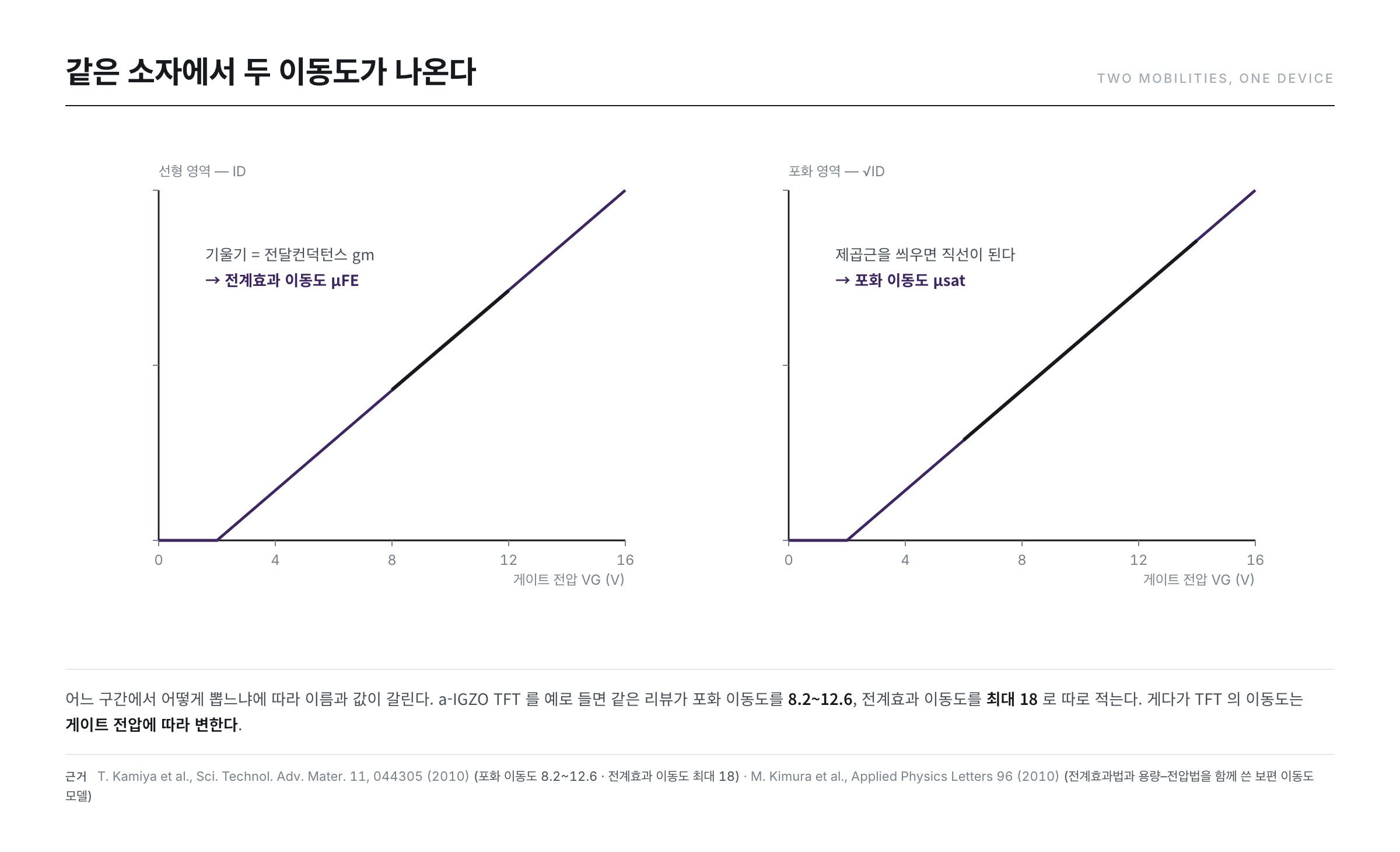
The point to note is that mobility is not a single number. Its name and value differ depending on which region it is extracted from and how.
- Field-effect mobility (μFE) — extracted from the slope of the curve (transconductance) in the linear region.
- Saturation mobility (μsat) — extracted from the slope of the straight line of √ID versus VG in the saturation region.
The same device gives different values. Even the 2010 review by Kamiya et al. cited above lists the saturation mobility of a-IGZO TFTs as 8.2–12.6 cm²V⁻¹s⁻¹ and the field-effect mobility separately as up to 18 cm²V⁻¹s⁻¹.
Moreover, the mobility of a TFT changes with gate voltage. The more electrons are gathered, the more the defect puddle is filled, and the remaining electrons move more freely. The study that Kimura et al. reported in Applied Physics Letters in 2010 confronts this problem head-on: the paper itself raises the issue that "different mobility models have been applied to different films", and reports that by combining the field-effect method with the capacitance–voltage method it obtained a universal mobility model. It further writes that the characteristics of a-IGZO TFTs that underwent different heat treatments are reproduced by the same mobility model with only the defect density changed.
To sum up — when looking at a mobility number, one must also look at which method and which conditions it was extracted under. Comparing mobility alone, without conditions, means little.
The fourth number — on/off current ratio
The on/off ratio (Ion/Ioff) is the current in the on state divided by the current in the off state. It expresses how firmly the switch closes.
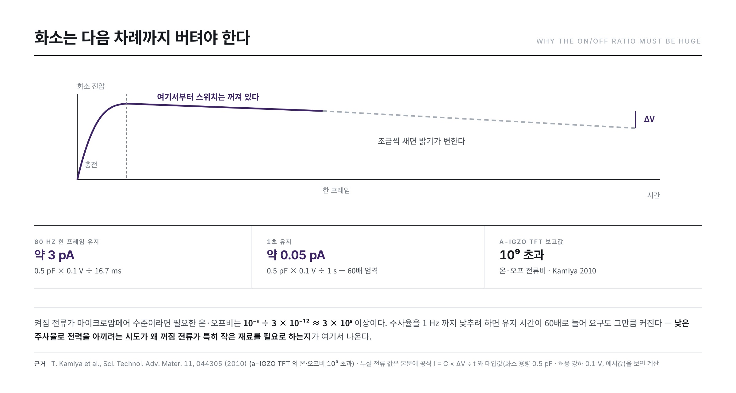
Why this value matters on a screen becomes clear when one thinks about how a pixel operates. A pixel must hold the voltage it was charged to until its next turn comes, and if the transistor leaks a little in the meantime, the voltage drains away and the brightness changes. The smaller the off current, the longer it holds.
The 2010 review by Kamiya et al. cited above reports that the on/off ratio of a-IGZO TFTs exceeds 10⁹. That means the on current is a billion times the off current.
Why this number has to be so large is shown by a simple calculation. Taking the pixel capacitance as 0.5 pF, the allowable voltage drop as 0.1 V, and the time to be held as one 60 Hz frame, 16.7 ms (all example values chosen to show the calculation), the allowable leakage current is
I = C × ΔV ÷ t = 0.5 pF × 0.1 V ÷ 16.7 ms = 5 × 10⁻¹⁴ ÷ 1.67 × 10⁻² ≈ 3 × 10⁻¹² A = about 3 pA
. If the on current is at the microampere level, the required on/off ratio is roughly 10⁻⁶ ÷ 3 × 10⁻¹² ≈ 3 × 10⁵ or more. If one then tries to lower the refresh rate not to 60 Hz but down to 1 Hz, the hold time becomes 60 times longer, so the required on/off ratio grows by the same factor — this is where it emerges why attempts to save power with a low refresh rate need a material with an especially small off current.
What it means when the curve flattens
We have looked at the four numbers one by one, but when actually reading a curve, changes in its shape tell you more.
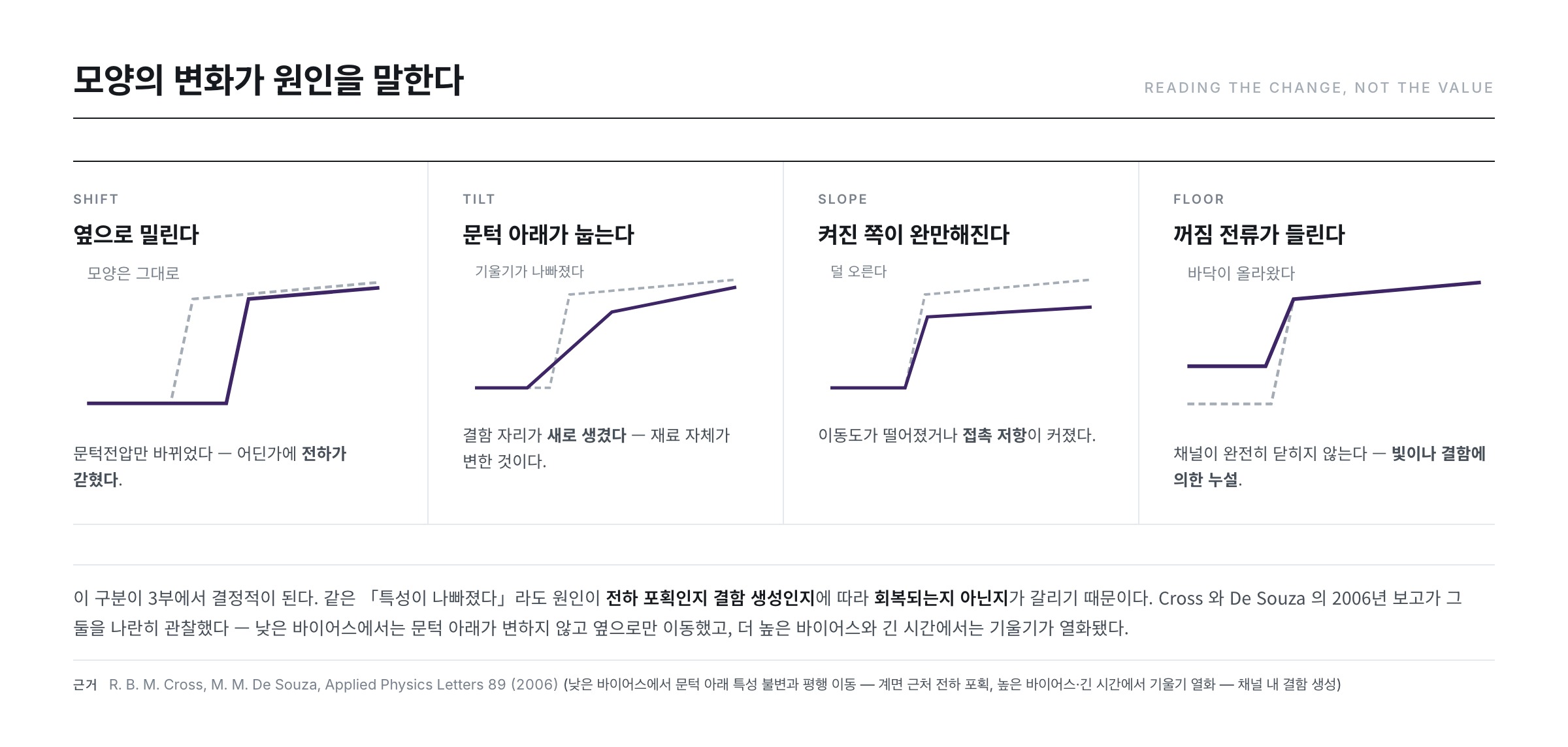
| Change in the curve | What it means |
|---|---|
| The whole curve shifts sideways in parallel | Only the threshold voltage has changed — charge has been trapped somewhere |
| The subthreshold section flattens (SS increases) | Defect sites have been newly created |
| The slope on the on side becomes gentler | Mobility has dropped or contact resistance has grown |
| The off current lifts | The channel does not close completely — leakage due to light or defects |
Why this distinction matters will become apparent in Section 3. Even for the same "characteristics have degraded", whether or not it recovers depends on whether the cause is charge trapping or defect creation.
To cite one real report in advance, the ZnO TFT stability study that Cross and De Souza published in Applied Physics Letters in 2006 observes two things side by side — under low bias stress the subthreshold characteristics do not change and the curve only shifts sideways, whereas under higher bias and longer time the subthreshold slope degrades. The paper attributes the former to charge trapping near the channel/insulator interface and the latter to defect state creation within the ZnO channel. The shape of the curve separated the causes.
In summary
- From a single curve come four numbers: threshold voltage, subthreshold swing, mobility, and on/off ratio.
- The subthreshold swing has a calculable lower limit at room temperature of about 59.5 mV/decade.
- Mobility is not a single number — it varies with the extraction method and the gate voltage.
- The required on/off ratio is calculated from how long the pixel must hold its voltage.
- Whether the curve shifts sideways or flattens separates the causes.
The next part deals with where the shape of this curve comes from — we set up the transistor's current equation ourselves and see why the linear region and the saturation region diverge.
References
- T. Kamiya, K. Nomura, H. Hosono, "Present status of amorphous In–Ga–Zn–O thin-film transistors," Sci. Technol. Adv. Mater. 11, 044305 (2010) : S value of about 100 meV/decade for a-IGZO TFTs, on/off ratio exceeding 10⁹, saturation mobility 8.2–12.6 and field-effect mobility up to 18 cm²V⁻¹s⁻¹
- M. Kimura et al., "Intrinsic carrier mobility in amorphous In–Ga–Zn–O thin-film transistors determined by combined field-effect technique," Applied Physics Letters 96 (2010) : raises the problem that different mobility models had been applied to different films; a universal mobility model combining the field-effect and capacitance–voltage methods; devices with different heat treatments reproduced by the same model with only the defect density changed
- R. B. M. Cross, M. M. De Souza, "Investigating the stability of zinc oxide thin film transistors," Applied Physics Letters 89 (2006) : parallel shift with unchanged subthreshold characteristics under low bias, degradation of subthreshold slope under high bias and long time — distinction between charge trapping and defect creation
- M. J. Powell, "The physics of amorphous-silicon thin-film transistors," IEEE Trans. Electron Devices 36, 2753 (1989) : the distinction that deep states determine the threshold voltage and conduction-band tail states determine the field-effect mobility