The previous series, "From Semiconductors to Transistors," followed the principles of the device. It set out from the band gap, built a PN junction, opened a channel with the field effect, and arrived at the cutoff, linear and saturation regions of operation. This series begins one step further along — the work of extracting numbers from a device that has already been built.
Evaluating a device comes down to measuring curves and reading values off them. Threshold voltage, mobility, slope, leakage current: all of them are obtained that way. Over eight installments this series takes up, one at a time, which curve to measure, how to measure it, and what value to read from it. The first installment is the very first picture anyone draws, the output curve.
The question is a simple one. Once a transistor has been built, how do you confirm that it behaves like a transistor? The first step is to raise the drain voltage while measuring the current. The result is the output curve, and what this single picture does and does not reveal is the subject of this installment.
The operating values in this text are examples chosen to show the calculation, not the specifications of any particular company. Every figure quoted has been verified in the public literature, and the sources are listed at the end.
Why the MOSFET equations carry over unchanged
A word about terminology first. The Wikipedia article "Thin-film transistor" defines a TFT (Thin-Film Transistor) as a kind of field-effect transistor (FET) made by thin-film deposition. What sets it apart from an ordinary MOSFET, where the silicon wafer itself serves as the substrate, is that it is placed on a supporting substrate that does not conduct electricity, such as glass.
The materials and the fabrication differ, but the mechanism of operation is the same field effect. The Wikipedia article "Field-effect transistor" defines an FET as a device that controls the current in a semiconductor with an electric field. That is why the equations and curve shapes used in this article are taken straight from the MOSFET literature.
How the measurement is made — hold one, sweep the other
A transistor has three terminals: the gate (G), the source (S) and the drain (D). That leaves two voltages.
- VGS — the voltage between gate and source. It decides how far the channel is held open.
- VDS — the voltage between drain and source. It decides how hard charge is pushed through the open channel.
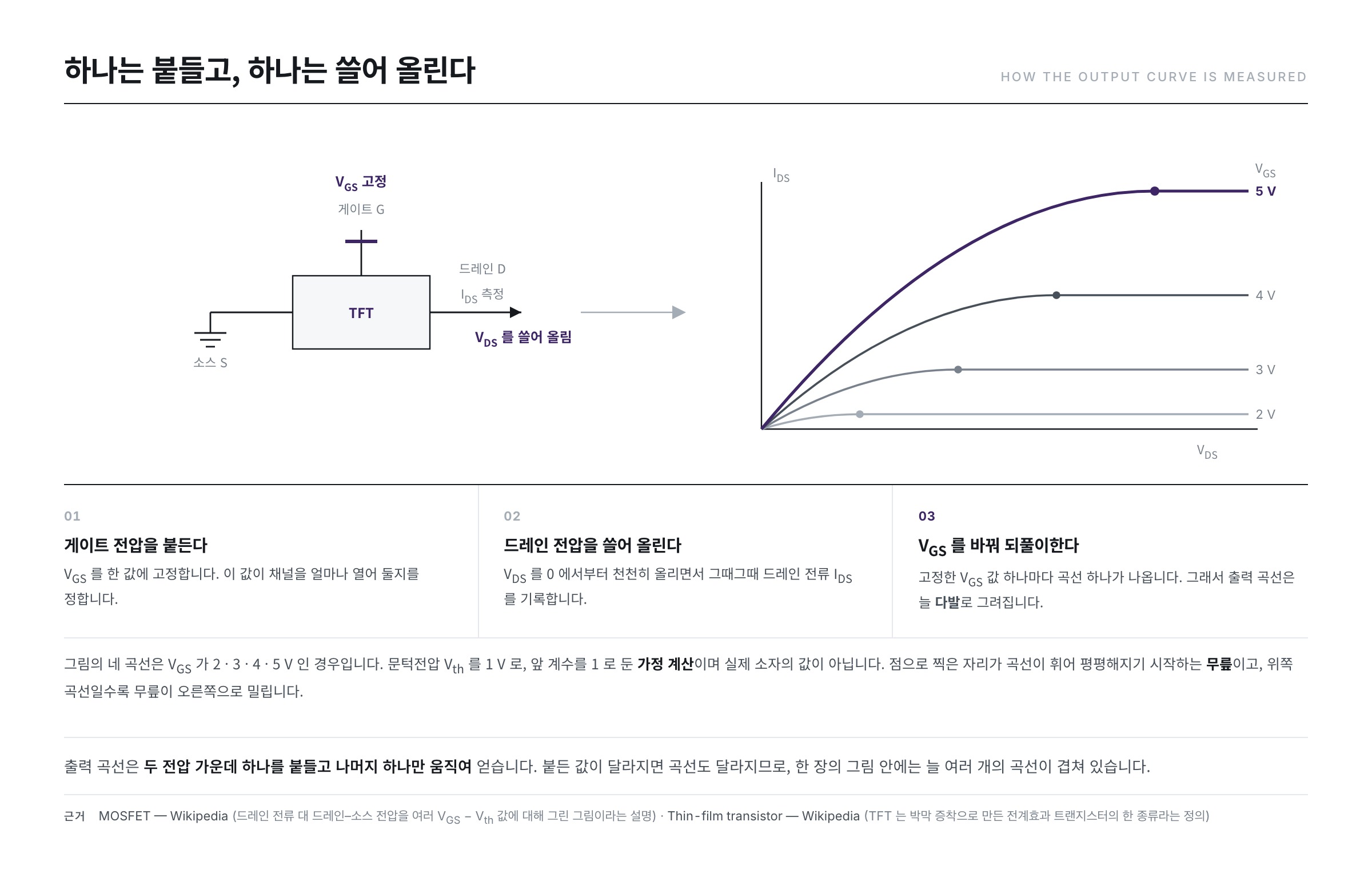
There is a single quantity to measure, the current flowing into the drain, IDS. But when two knobs govern the current, one picture cannot hold them both. So one knob is held fast and only the other is moved.
The output curve is the record of holding VGS at one value and sweeping VDS up from zero while logging IDS. That gives one curve. Change the fixed VGS value and sweep again, and another appears. This is why an output curve is always drawn as a family of overlapping traces.
The output-curve figure carried in the Wikipedia article "MOSFET" is captioned in the same terms — drain voltage against drain current, drawn for several values of VGS − Vth.
Inside a single curve — slope, knee, plateau
Let us follow one curve from left to right. It passes through three regions.
The slope — where the device behaves like a resistor
Near the origin the current grows almost in proportion to the drain voltage. The "MOSFET" article calls this the triode region, also known as the linear or ohmic region, and states the condition as follows.
VGS > Vth and VDS < (VGS − Vth)
For this region the "MOSFET" article describes the device as behaving like a resistor whose value is set by the gate voltage, and writes the current as follows.
ID = μnCox (W/L) [ (VGS − Vth)VDS − VDS2/2 ]
Look inside the bracket and the proportionality becomes visible. When VDS is very small, the trailing VDS2/2 term is negligible beside the leading one. The current is then simply proportional to VDS, and what fixes the slope is (VGS − Vth). Rewritten as a resistance, it reads as follows.
R ≈ 1 / [ μnCox(W/L)(VGS − Vth) ]
Push the gate twice as far above the threshold and the resistance halves. The switch that turns a pixel on the screen on and off operates in this region.
The knee — its position is set by the gate
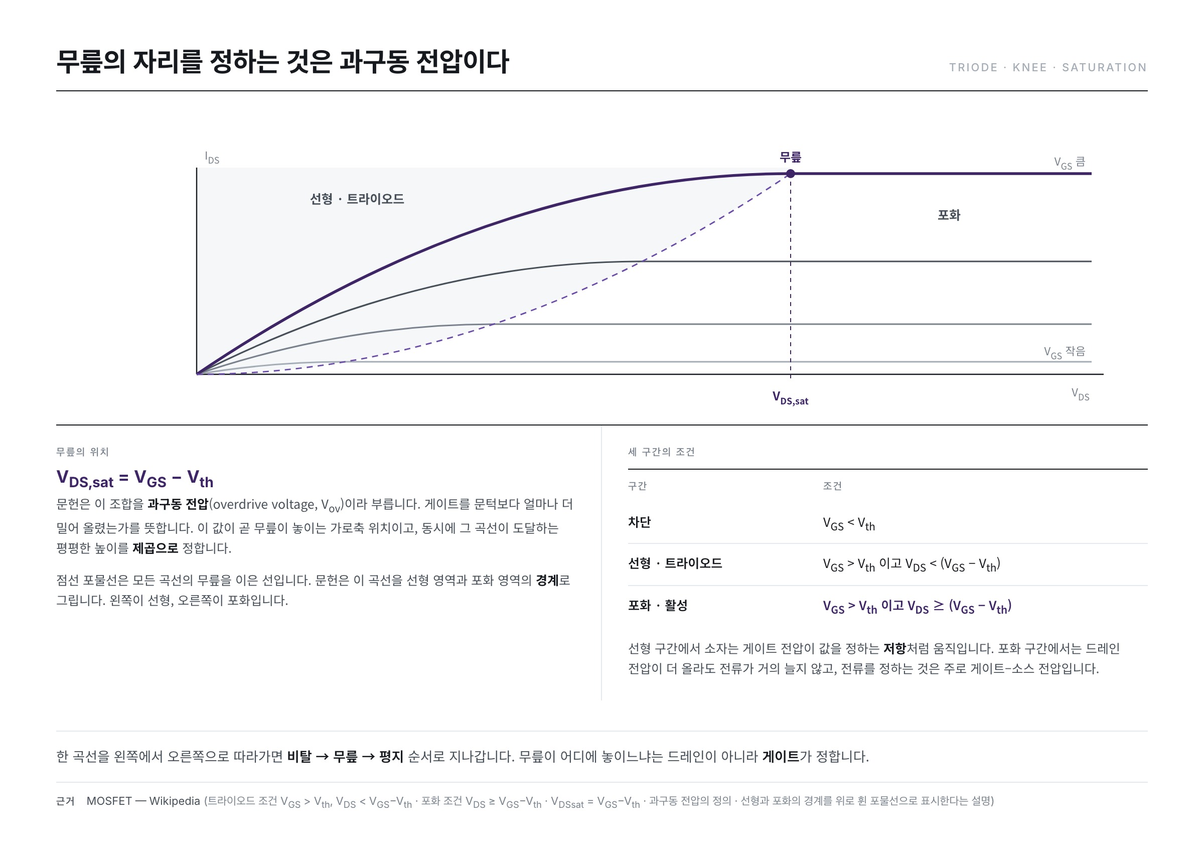
Keep raising VDS and the curve bends over and flattens out. The place where it bends is called the knee. The knee sits here.
VDS,sat = VGS − Vth
The "MOSFET" article calls this combination Vov = VGS − Vth the overdrive voltage (the amount by which the gate has been pushed past the threshold). Here lies the most important point in the whole picture. Where the knee lands is decided by the gate, not by the drain. However carefully the drain voltage is swept, the position of the knee does not move.
The plateau — where the drain lets go
Past the knee comes the saturation, or active, region. The condition is the reverse of the triode one.
VGS > Vth and VDS ≥ (VGS − Vth)
The "MOSFET" article calls the onset of this region pinch-off. It means the channel has vanished at the drain end. Even though the channel no longer spans the full length of the device, the electric field between drain and channel is so large that conduction continues. And it puts it this way — the drain current now depends only weakly on the drain voltage and is set chiefly by the gate-source voltage.
That one sentence is the entire reason a transistor can serve as an amplifier. Because the current does not swing along with the output voltage, only the small signal placed on the gate is carried through faithfully.
Between the curves — the spacing widens as a square
Now look at the whole family rather than a single curve. The higher the curve, the larger the VGS that was held fixed and the higher the plateau. So far this is obvious. What matters is the way the spacing widens.
The current in the saturation region is written as follows.
ID = (μnCox/2)(W/L) (VGS − Vth)2 (1 + λVDS)
There is a square in it. This article computes with Vth taken as 1 V, the leading coefficient (μnCox/2)(W/L) taken as 1, and the final bracket taken as 1 for the moment. These are not the values of a real device but assumptions made solely to expose the ratios.
- VGS = 2 V → overdrive 1 V → knee 1 V, saturation current 1
- VGS = 3 V → overdrive 2 V → knee 2 V, saturation current 4
- VGS = 4 V → overdrive 3 V → knee 3 V, saturation current 9
- VGS = 5 V → overdrive 4 V → knee 4 V, saturation current 16
The gate voltage was raised in even steps of 1 V, yet the gaps in current widen to 3, 5 and 7. The very fact that the family thins out toward the top is the evidence of a square-law relation. Set that against the knee, which slides evenly to the right at 1, 2, 3 and 4 V — the knee is first order, the height is second order.
The literature states the same thing in terms of a slope. The transconductance given in the "MOSFET" article is gm = 2ID / Vov. It expresses how much the current changes for a small change in gate voltage, which is to say how much the device amplifies a signal. On an output curve this quantity shows up as the spacing between curves, and the next installment treats it properly.
The plateau is not perfectly flat
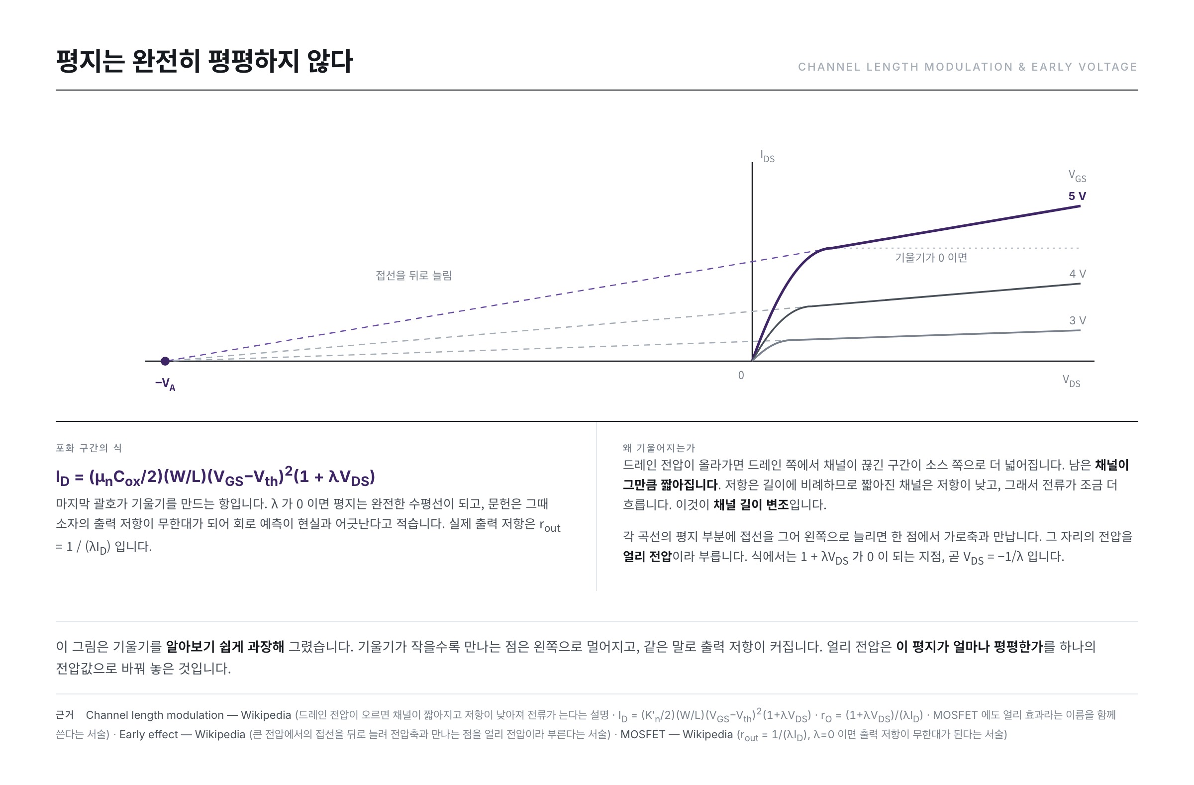
Measure a real device and the saturation region is not a horizontal line but tilts very slightly upward to the right. The (1 + λVDS) that was set to 1 a moment ago is that tilt.
The reason is explained by the article "Channel length modulation". As the drain voltage rises, the influence of the drain reaches further toward the source, the stretch where the channel is broken grows wider, and the length of the remaining channel gets shorter. Resistance is proportional to length, so the shortened channel has a lower resistance and a little more current flows. This is called channel length modulation. The "Channel length modulation" article adds that the effect becomes more pronounced the shorter the source-drain spacing, the deeper the drain junction and the thicker the insulating film.
Written as a single voltage, the slope is the Early voltage
There is a way to put the slope of the plateau into a single number. Draw a tangent to the plateau, extend it far to the left, and look at the point where it meets the horizontal axis. The Wikipedia article "Early effect" defines it in exactly that way — the voltage at which the tangent taken at large voltage, extended backward, meets the voltage axis is called the Early voltage (VA).
It also falls straight out of the equation. The point at which (1 + λVDS) becomes 0 is VDS = −1/λ. That is where the tangent meets the horizontal axis. The smaller the slope λ, the further away the meeting point lies, and the flatter the plateau is.
Written as a resistance, the same quantity is the output resistance in the "MOSFET" article, rout = 1 / (λID). The article notes that setting λ to 0 makes the output resistance infinite and puts circuit predictions at odds with reality. The tilt of the plateau is not a flaw that ought not to be there but a value circuit design must know.
The name came originally from the bipolar transistor (BJT). The "Early effect" article puts the Early voltage of a BJT in the range 15~150 V and adds that it grows smaller as the device grows smaller. The "Channel length modulation" article states that because the way it appears in the current is similar, the same name is used for the MOSFET as well. The value quoted by the "Channel length modulation" article, however, is a fitting coefficient of the form λ ≈ ΔL / (VEL), and it gives VE ≈ 4 V/μm for a 65 nm process as an example. A different device structure gives a different magnitude, so this installment goes no further than the concept.
What the output curve does not tell you
This is as far as the output curve goes. Does the channel open, is there a region that behaves like a resistor, is there a knee, how flat is the plateau. For confirming that the device behaves like a transistor, that is enough.
Yet among the values used in evaluating a device there are some that cannot be read off this picture directly. There are three of them.
- Threshold voltage Vth — the knee of an output curve tells you VGS − Vth and no more; it does not hand over Vth on its own. The Wikipedia article "Threshold voltage" defines Vth as the minimum gate-source voltage needed to create a conducting path between source and drain, and states that in practice it is specified as the point at which a current of a fixed size flows, 250 μA or 1 mA for instance. Either way it is a value that emerges only when the gate voltage is swept.
- Mobility μn — in the saturation equation μn enters as a single coefficient, multiplied by Cox and W/L. There is no way to split that product on a single output curve and take out the mobility alone.
- Leakage current — even in the cutoff region, where VGS falls short of Vth, the current is not zero. The "MOSFET" article states that this subthreshold current varies exponentially with gate voltage, in the form ID ≈ ID0 e(VGS − Vth) / nVT. It is smaller by orders of magnitude, so on an output curve with a linear vertical axis it lies flat against the bottom and cannot be seen.
They have one thing in common. All three are values that appear only when the knob being held fast, the gate voltage, is moved. Because the output curve holds the gate fixed, it cannot carry that information at all.
Summary
- The output curve is the picture obtained by holding VGS fixed and sweeping VDS while logging IDS. As many curves appear as there are fixed values, making a family.
- A single curve passes through linear (triode) → knee → saturation in that order. The knee sits at VDS,sat = VGS − Vth, and it is decided by the gate, not the drain.
- The spacing between curves widens as a square. Raise the gate in even steps of 1 V and the saturation current jumps 1, 4, 9, 16.
- The saturation region is not perfectly flat because of channel length modulation. Extending the tangent to the left, the point where it meets the horizontal axis is the Early voltage, and written as a resistance the same quantity is rout = 1/(λID).
- Threshold voltage, mobility and leakage current cannot be read off this picture directly. The reason is that the gate was held fixed.
The next installment changes the axes. Hold the drain voltage and sweep the gate voltage upward — that is the transfer curve. The values just described as unreadable come out there.
References
- MOSFET — Wikipedia : the triode condition and its current equation; the saturation condition and its current equation ID = (μnCox/2)(W/L)(VGS−Vth)2(1+λVDS); pinch-off; the overdrive voltage Vov and VDSsat = VGS−Vth; gm = 2ID/Vov; rout = 1/(λID); the exponential relation of the subthreshold current; and the statement that the output curve is drawn for several values of VGS−Vth
- Channel length modulation — Wikipedia : the account that a rising drain voltage shortens the channel, lowers the resistance and increases the current; rO = (1+λVDS)/(λID); λ ≈ ΔL/(VEL) with the 65 nm process example VE ≈ 4 V/μm; and the statement that the name Early effect is used for the MOSFET as well
- Early effect — Wikipedia : the definition that the point where the tangent taken at large voltage, extended backward, meets the voltage axis is called the Early voltage; the BJT Early voltage range of 15~150 V and the statement that it grows smaller as the device grows smaller
- Thin-film transistor — Wikipedia : the definition that a TFT is a kind of field-effect transistor made by thin-film deposition and is built on a substrate that does not conduct electricity, such as glass
- Field-effect transistor — Wikipedia : the definition of an FET as a device that controls the current in a semiconductor with an electric field, and the account that it acts like a variable resistor at low drain voltage and like a constant-current source in saturation
- Threshold voltage — Wikipedia : the definition of the threshold voltage as the minimum gate-source voltage that creates a conducting path between source and drain, and the account that it is specified by a current of a fixed size (250 μA or 1 mA)
- ※ Passages quoted from the Wikipedia articles in the list above are under the CC BY-SA 4.0 license.