In the previous part we saw six ways a curve goes off. One of them was the whole curve sliding sideways. This part follows one of the causes of that slide all the way through.
The starting point is a slightly odd fact. Threshold voltage is a value the gate decides. How much has to be applied to the gate to open the channel — that value is the threshold voltage. And yet leave the gate alone, raise only the drain voltage, and the threshold voltage comes down.
The drain is the side the current leaves by. Opening and closing the door is the gate's job. And yet the drain interferes with the gate's work. How that happens is the question of this part.
The condition values in the text are examples chosen to show the arithmetic, not the specifications of any particular company. Every figure quoted has been verified in the public literature, and the sources are listed at the end.
Starting with the Name
The phenomenon has a name. It is DIBL (Drain-Induced Barrier Lowering). The four words are a sentence in themselves — a lowering, of the barrier, induced by the drain.
The Wikipedia article "Drain-induced barrier lowering" classifies it as one of the short-channel effects, and states that the term originally refers to the lowering of a transistor's threshold voltage at high drain voltage.
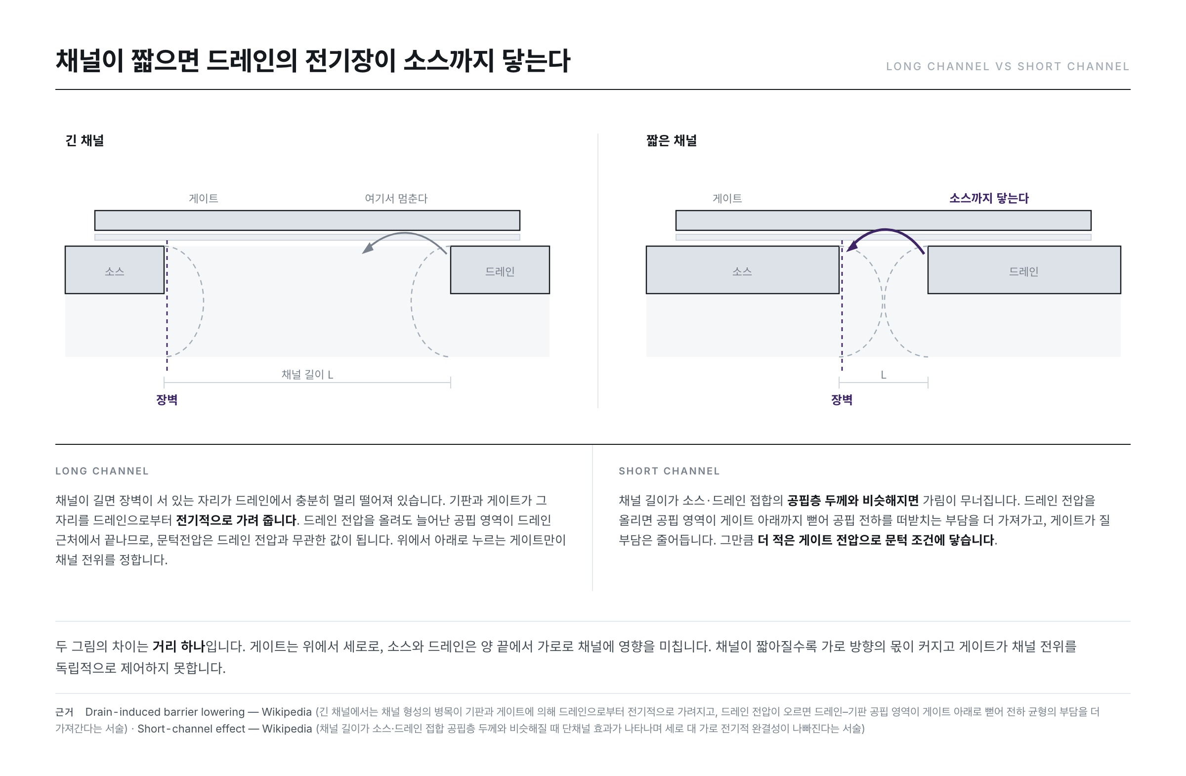
The DIBL article also notes why this does not happen in long-channel devices. When the channel is long, the bottleneck of channel formation sits far enough from the drain contact that the substrate and the gate screen that spot electrically from the drain. So the threshold voltage was a value independent of drain voltage. As the channel shortens, that screening breaks down. The drain comes close enough to touch the channel, and a high drain voltage opens the bottleneck and turns the transistor on earlier than intended.
Let us first look at what the "barrier" in the name is. Understand that word and the rest follows.
The Barrier — the Hill a Carrier Has to Climb
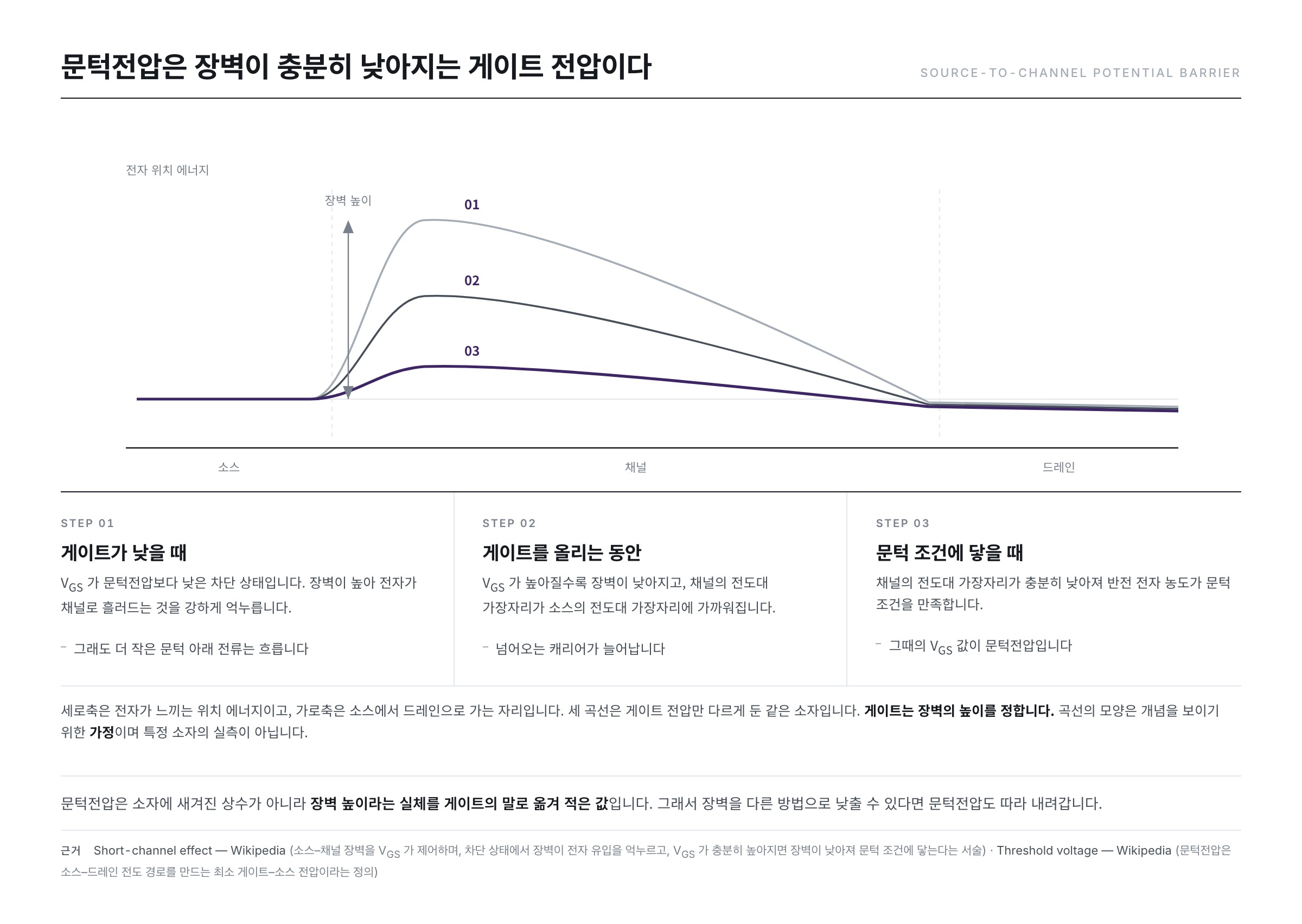
Carriers do not simply drift back and forth between source and drain. Between them there is a hill to be climbed. Put electrically, it is the potential barrier between the source and the channel.
The Wikipedia article "Short-channel effect" treats this barrier head-on. In a planar long-channel n-type device, it states, what controls the barrier between source and channel is the gate-source voltage VGS. And it continues like this.
- In the cutoff state, where VGS is lower than the threshold voltage, this barrier strongly suppresses the flow of electrons into the channel. A smaller subthreshold current can still flow, however.
- Once VGS becomes high enough, the barrier is lowered, and the conduction band edge of the channel approaches that of the source.
- When the channel's conduction band edge has fallen enough that the inversion electron concentration satisfies the threshold condition, the value of VGS at that moment is the threshold voltage.
Here the meaning of threshold voltage gains a layer. The Wikipedia article "Threshold voltage" defines it as the minimum gate-source voltage needed to create a conducting path between source and drain. Rendered in the language of the barrier, the same meaning reads like this — the gate voltage at which the barrier becomes low enough.
The threshold voltage is not a constant engraved in the device. There is a real thing called barrier height, and the threshold voltage is the voltage record of how far the gate pushes that real thing down. If the barrier can be lowered by some other means, the threshold voltage comes down along with it. That sentence is the key to this whole part.
The Drain Lays a Hand on the Barrier
Now leave the gate alone and raise only the drain voltage.
The same Wikipedia DIBL article explains the reason in terms of charge neutrality. The combined amount of charge in the device's depletion region and charge in the channel is held up jointly by the charges on the three electrodes — gate, source and drain. Raising the drain voltage enlarges the depletion region of the pn junction between drain and substrate, so that it reaches in under the gate. By that much, the drain takes on more of the burden of supporting the depletion charge, and the burden the gate has to carry is reduced.
The burden has fallen, yet the charge on the gate is unchanged. That charge then draws more carriers into the channel in order to balance. The article states that this is the same effect as having lowered the threshold voltage of the device.
Rendered in the language of the barrier, the same event reads like this — the channel becomes a more attractive place for electrons. In other words, the potential energy barrier seen by electrons in the channel is lowered. This is where the name "barrier lowering" comes from.
Distance Decides Everything
This does not happen everywhere. The Wikipedia "Short-channel effect" article states the boundary clearly. Short-channel effects appear when the channel length becomes comparable to the depletion layer thickness of the source and drain junctions.
The "Short-channel effect" article explains the situation with forces in two directions.
- The vertical direction — the gate controls the channel from above.
- The lateral direction — the source and the drain influence the channel from the two ends.
When the channel is long, the middle sits far from both ends and the lateral influence does not reach it. The gate takes that spot on alone. As the channel shortens, the middle is no longer isolated from the influence of source and drain, and the gate cannot control the channel potential either independently or uniformly. The article gives this property the name electrostatic integrity, and states that the shorter the channel, the worse it gets.
The Wikipedia article "MOSFET" puts the same story more briefly. Because of short-channel effects, channel formation is not carried out entirely by the gate; the drain and the source take part in it too. Raising VDS enlarges the depletion region, and since a considerable amount of charge is depleted by VDS, the gate voltage needed to form the channel becomes lower.
On the Curve It Looks Like Two Lines Side by Side, Offset
Now back to the measurement screen. In part 2 of the previous series we said that a transfer curve always carries a note of where the drain voltage was set. This is the reason.
The Wikipedia DIBL article sets out in stages how DIBL shows up in the subthreshold region as the channel length shrinks.
- At first it appears as the whole subthreshold current versus gate voltage curve shifting in parallel with changes in drain voltage. This stage can be modeled as a simple change of threshold voltage with drain voltage.
- As it gets shorter, the slope of the curve itself is reduced. A larger change in gate voltage becomes necessary to obtain the same change in current.
- When it becomes extremely short, the gate fails outright to turn the device off. This stage is not explained by adjusting the threshold voltage alone.
The first item is the previous part's "lateral shift," and the second is its "slope laying down." It means the two shapes counted separately in the previous part can come from the same root.
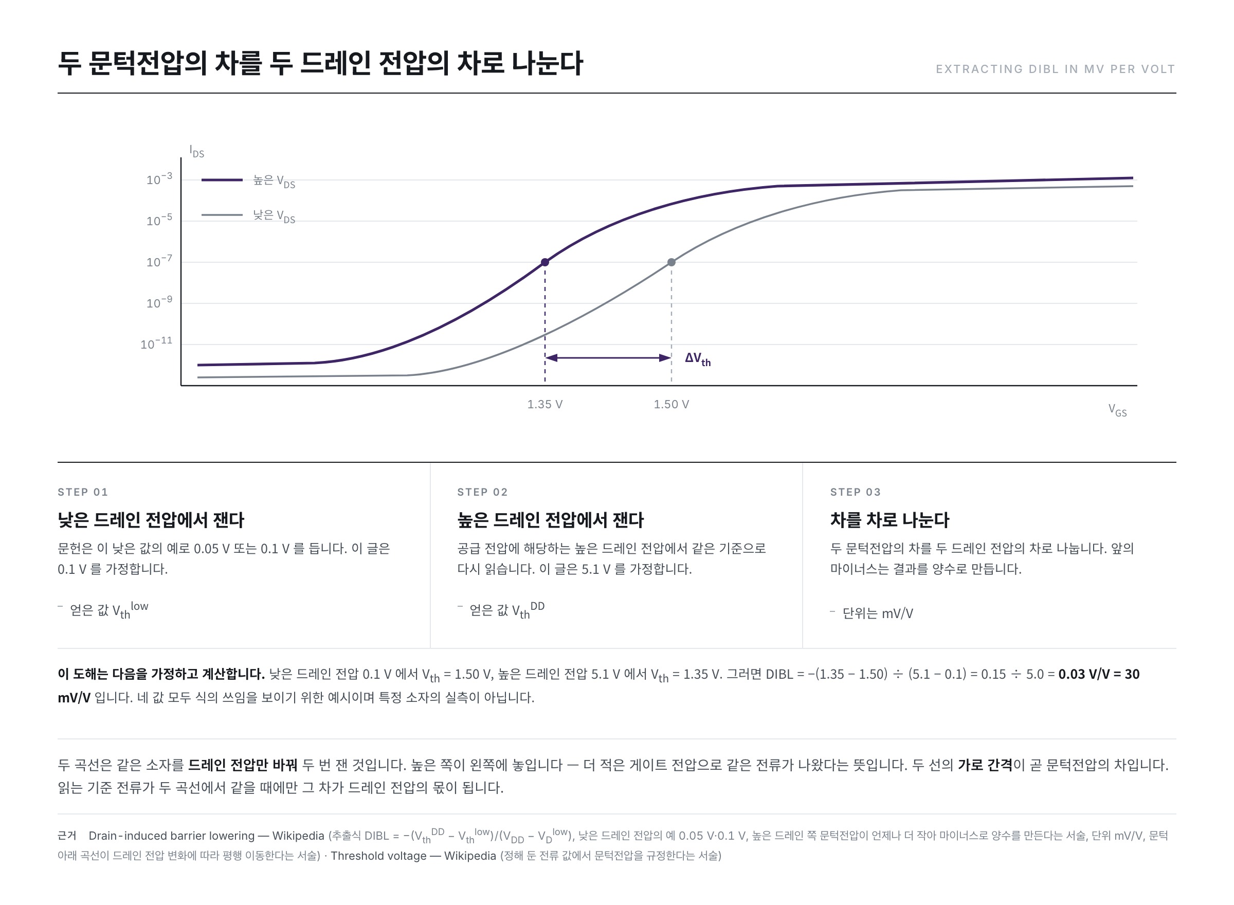
So if a transfer curve measured at a low drain voltage and one measured at a high drain voltage are drawn on the same sheet, the two lines sit side by side and offset. The high one is on the left. It means the same current came out with less gate voltage, which means the threshold voltage has come down by that much.
The same drain voltage influence appears on the on side as well. The DIBL article states that it also affects the current versus drain voltage curve in the active region, so that as the drain voltage rises the current increases and the output resistance falls. And it makes clear that the ordinary effect of channel length modulation on output resistance has this share added on top of it. The reason the right-hand side of the output curve was not perfectly flat in the previous series was not a single one.
How to Write It as a Number
"The curve has shifted" is not something with which two devices can be compared. So the extent of the shift is written as a single number.
The method is simple. Measure the threshold voltage at each of two drain voltages, and divide their difference by the difference in drain voltage. The expression carried in the Wikipedia DIBL article is this.
DIBL = − ( VthDD − Vthlow ) / ( VDD − VDlow )
The meaning of each symbol is written down in the DIBL article as well.
- VthDD — the threshold voltage measured at the high drain voltage (the supply voltage)
- Vthlow — the threshold voltage measured at a very low drain voltage. The article gives 0.05 V or 0.1 V as examples of such a low value
- The minus sign at the front — it is there to make the result positive. The threshold voltage on the high-drain side is always smaller than on the low-drain side
The unit is mV/V. It is a value read as "how many mV the threshold voltage comes down for each 1 V rise in drain voltage."
This article puts the low drain voltage at 0.1 V and the high one at 5.1 V, and calculates on the assumption that the threshold voltages read there are 1.50 V and 1.35 V respectively. All four values are examples chosen to show how the expression is used.
DIBL = − ( 1.35 − 1.50 ) / ( 5.1 − 0.1 ) = 0.15 / 5.0 = 0.03 V/V = 30 mV/V
There is one hidden assumption in this expression. It is where the threshold voltage was read. As seen in the previous series, a transfer curve has no sharp kink, so the threshold voltage is a value fixed by setting up a definition. The Wikipedia "Threshold voltage" article states that datasheets specify the threshold voltage at a chosen measurable current value, and gives 250 μA and 1 mA as examples. Only when both curves are read by the same criterion does their difference become the drain voltage's share.
The DIBL article also carries a relation connecting this number to the operating speed of a circuit.
Δf / f = − 2 · DIBL / ( VDD − Vth )
Putting in the values assumed above, VDD is 5.1 V and Vth is 1.35 V, so −2 × 0.03 ÷ 3.75 = about −0.016, a share of 1.6 %. It is an expression showing that a curve shifting does not end inside the curve.
What Channel Length Decides
DIBL has a different value from device to device. What sets its size is already contained in the explanation above — it is distance.
The Wikipedia DIBL article states that the barrier lowering grows as the channel length shrinks. And it adds, interestingly, that this holds even when no drain bias is applied at all. The source and the drain each form a pn junction with the substrate, and such a junction comes with a built-in depletion layer even without a reverse voltage applied. When the channel is short, this built-in depletion layer alone intervenes meaningfully in the charge balance.
Here a twin phenomenon with a different name appears. The Wikipedia "Short-channel effect" article separates the two like this.
- Threshold voltage roll-off — observed by shortening the channel length while holding the drain-source voltage fixed. It speaks of how the threshold voltage depends on channel length.
- DIBL — observed by raising VDS while holding the channel length fixed. It speaks of how the threshold voltage depends on drain voltage.
The article states that the two come from the same root, the loss of electrostatic integrity, and that only the variable being changed differs. So the short-channel effect seen in the previous series and the DIBL of this part were not two separate subjects.
Push Further and It Is Punch-Through
We said the drain's depletion region reaches in under the gate. A natural question then arises — what happens if it keeps reaching.
There is a depletion region on the source side too. The two grow toward each other, and there is a point at which they meet. The name given to that state is punch-through.
The patent US8476684B2, published on Google Patents, defines the state like this. Punch-through occurs when the sum of the width of the depletion region around the drain (extending toward the source) and the width of the depletion region around the source (extending toward the drain) equals the source-drain spacing, so that a continuous depletion region runs from source to drain.
Another published patent, US5973363A, writes down where the electric field is at that moment. The contours of the lateral electric field do not terminate in the gate channel region but extend between the source and the drain. And this happens mainly in the bulk region, further removed from the field control exercised by the voltage on the gate.
DIBL and punch-through are not different events. They are a difference of degree. When the drain's influence reaches the barrier on the source side and lowers it a little, it looks like the threshold voltage has come down; when that influence grows all the way and the two depletion regions join, there is nothing left for the gate to handle. The last stage of the DIBL article seen earlier — the statement that at extremely short lengths the gate fails outright to turn the device off — points to the same place.
Examples of pulling this distance apart by structure are on record in the literature as well. The Wikipedia "MOSFET" article introduces the FinFET as one of several geometries brought in to mitigate short-channel influence and reduce DIBL. Control lost on the plane was regained by standing the channel up and wrapping the gate around it.
Summary
- Between source and channel there is a potential barrier for carriers to climb, and the gate sets its height. The threshold voltage is the gate voltage at which the barrier becomes low enough.
- Raising the drain voltage makes the drain's depletion region reach in under the gate and share the burden of the depletion charge. To the extent the gate's burden is reduced, less gate voltage reaches the threshold condition — the threshold voltage has come down.
- On the curve it looks like a low-VDS curve and a high-VDS curve side by side and offset. As it gets shorter the slope lies down as well, and at the extreme the gate fails to turn it off.
- As a number it is written in mV/V by dividing the difference of the two threshold voltages by the difference of the two drain voltages. The sign is flipped because the value on the high-drain side is always the smaller one.
- It grows as the channel gets shorter, and appears from the built-in depletion layer alone even when the drain bias is 0. When it grows all the way and the two depletion regions join, it is punch-through, and the two are a difference of degree.
This part looked at the path by which the drain pulls the threshold down. The next part moves, at the same drain location, to a path along which the gate instead produces leakage on the off side — GIDL.
References
- Drain-induced barrier lowering — Wikipedia : the definition of DIBL and its classification as a short-channel effect, the statement that in a long channel the bottleneck is electrically screened from the drain, the charge neutrality (Yau charge sharing) explanation, the stages in the subthreshold region running from parallel shift through slope reduction to failure of cutoff, the reduction of active-region output resistance, the extraction expression DIBL = −(VthDD − Vthlow)/(VDD − VDlow) and the unit mV/V, the examples 0.05 V and 0.1 V for the low drain voltage, the frequency relation Δf/f = −2·DIBL/(VDD − Vth), and the statement that barrier lowering grows as the channel length shrinks even at zero drain bias
- Short-channel effect — Wikipedia : the definition that short-channel effects appear when the channel length becomes comparable to the depletion layer thickness of the source and drain junctions, the statement that VGS controls the source-channel barrier and the sequence of cutoff, barrier lowering and threshold condition, vertical (gate) versus lateral (source and drain) electrostatic integrity, and the distinction that threshold voltage roll-off and DIBL share the same root and differ only in the variable being changed
- Threshold voltage — Wikipedia : the definition of threshold voltage as the minimum gate-source voltage creating a source-drain conducting path, and the statement that datasheets specify the threshold voltage at a chosen current value (for example 250 μA or 1 mA)
- MOSFET — Wikipedia : the explanation that short-channel effects make the drain and source take part in channel formation and that a rise in VDS lowers the gate voltage needed to form the channel, and the statement that the FinFET is one of the geometries introduced to mitigate short-channel influence and reduce DIBL
- Channel length modulation — Wikipedia : the statement that DIBL is the drain's influence in the weak inversion region acting similarly to channel length modulation and thereby degrading the cutoff characteristics
- US8476684B2 — Field effect transistors having improved breakdown voltages and methods of forming the same (Google Patents) : the definition that punch-through occurs when the sum of the source and drain depletion region widths equals the source-drain spacing so that a continuous depletion region runs between them
- US5973363A — CMOS circuitry with shortened P-channel length on ultrathin silicon on insulator (Google Patents) : the statement that under punch-through the lateral field contours do not terminate in the gate channel region but extend between source and drain, occurring mainly in the bulk region far from the gate voltage's field control
- ※ The portions quoted from Wikipedia articles in the list above are licensed under CC BY-SA 4.0.