Once photolithography is finished, what sits on the substrate is a circuit shape drawn in photoresist (PR). But that is only a picture. To become an actual circuit, the film not covered by PR has to be removed. That job belongs to etching, the step repeated more often than any other in backplane processing. As the opening instalment of the etch chapter, this post organises the shared concepts and parameters.
What etching is
Etching is the process of removing material selectively, chemically or physically. The heart of it is the word "selectively" — remove only what must go, and leave untouched both what must stay (under the PR) and the film underneath.
There are broadly two ways: wet etching, immersing or spraying with liquid chemicals, and dry etching, cutting with the reactive species of a plasma. Their characters are close to opposite.
Throw a stone, or spray water?
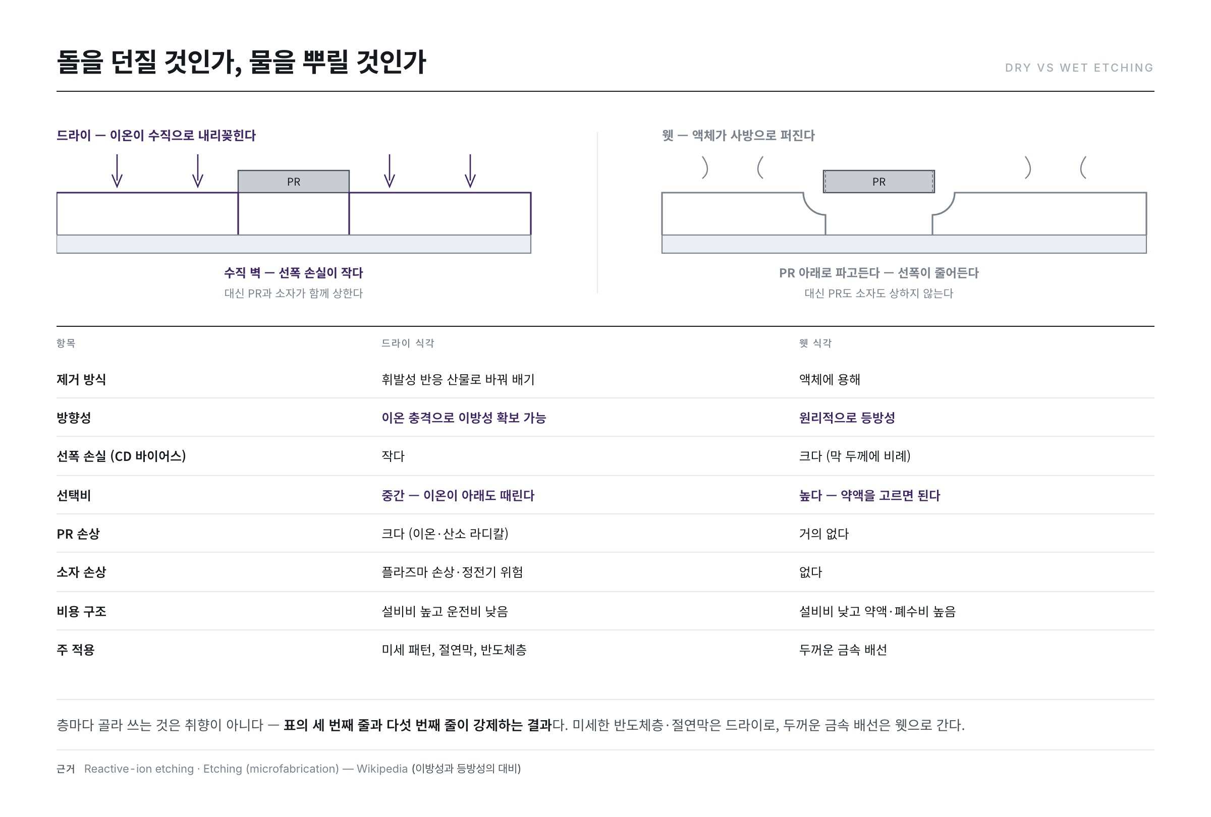
Here is an analogy. Suppose you must clear only the snow off a wooden board. Throw a stone and exactly the spot you hit is cleared — but the board is damaged too. Spray water and the board is fine, but the water spreads everywhere and melts snow you wanted to keep.
Dry etching is the stone, wet etching the water. Wikipedia puts the difference precisely — "RIE can produce very anisotropic profiles, in contrast to the typically isotropic profile of wet chemical etching" (Reactive-ion etching).
| Item | Dry etch | Wet etch |
|---|---|---|
| Removal mechanism | converted to volatile products, pumped away | dissolved in liquid |
| Directionality | anisotropy obtainable via ion bombardment | isotropic in principle |
| Line-width loss (CD bias) | small | large (scales with film thickness) |
| Selectivity | moderate — ions strike the underlayer too | high — choose the chemistry |
| PR damage | large (ions and oxygen radicals) | almost none |
| Device damage | plasma damage and ESD risk | none |
| Cost structure | high capital, low running cost | low capital, high chemical and waste cost |
| Main application | fine patterns, dielectrics, semiconductor layers | thick metal wiring |
So a real line chooses per layer: dry for fine semiconductor and dielectric layers, wet for thick metal wiring. That choice is not taste — it is forced by the third and fifth rows of the table.
Four rulers for measuring an etch
1. Etch rate
Thickness removed per unit time, usually in Å/min. If a 3,000Å film clears completely in 90 seconds, the rate is 33.3Å/s, that is 2,000Å/min. Faster means more throughput, but as a rule raising the etch rate degrades uniformity.
Etch rate is not a fixed constant but a function of conditions. Wherever chemistry is involved it is exponentially sensitive to temperature, and it also depends on the supply of reactive species and on pressure. That the rate changes substantially with temperature and exposed area, even in the same gas, was measured early on (Loading effect and temperature dependence of etch rate of silicon materials in CF4 plasma, 1980). This is why the assumption "same recipe, same result" does not hold.
2. Uniformity
How evenly the whole substrate is etched. It is commonly computed as
U = (max − min) ÷ (2 × mean) × 100 [%]
If the amount removed across the substrate is at most 2,200Å, at least 1,800Å, and 2,000Å on average, then U = 400 ÷ 4,000 = ±10%. Uniformity is examined at three levels — within-glass, glass-to-glass and lot-to-lot — and the level that wobbles points at a different cause (distribution inside the tool / transport and temperature / chemical and consumable life).
Within-substrate distribution usually appears as a centre-to-edge pattern. Plasma density and radical concentration tilt radially with reactor geometry, and that tilt becomes the etch distribution. Measurement and modelling of this distribution in a high-density plasma reactor shows the relationship (M. Surendra, C. R. Guarnieri, G. S. Selwyn, Appl. Phys. Lett. 66(18), 2415 (1995)).
3. Selectivity
The ratio between the etch rate of the target film and that of the film beneath it.
S = etch rate of target film ÷ etch rate of underlayer (or PR)
Ideally only the target is removed and the underlayer is untouched. To quote Wikipedia directly, "the ability of an etching system depends on the ratio of the etch rates of the two materials (the selectivity)" (Etching (microfabrication)). Low selectivity means cutting into the underlayer and ruining the device.
What matters is that selectivity is a designed value, set by gas chemistry. A classic 1978 experiment showed that adding oxygen bit by bit to a carbon tetrafluoride plasma moves the etch rates of silicon and of oxide in different directions, so the ratio between the two materials can be tuned by composition alone (C. J. Mogab, A. C. Adams, D. L. Flamm, J. Appl. Phys. 49(7), 3796 (1978)). Selectivity is not a constant handed down by the materials but a number the engineer makes.
4. Anisotropy
The ratio between lateral and vertical etch rates. Quantitatively it is defined as
A = 1 − (lateral etch rate ÷ vertical etch rate)
A = 0 is fully isotropic — cutting equally in all directions and undercutting the PR. A = 1 is fully anisotropic — cutting only downward, producing a vertical wall. The microfabrication literature treats this directionality as one axis of the coordinate system for choosing etch conditions, and shows that pressure, bias and gas composition move A (H. Jansen, M. de Boer, R. Legtenberg, M. Elwenspoek, J. Micromech. Microeng. 5(2), 115 (1995)).
Wikipedia sums it up: "etchants with a large bias are called isotropic, because they erode the substrate equally in all directions. Modern processes greatly prefer anisotropic etching, because they produce sharp, well-controlled features" (same article).
How line width is controlled — CD and bias
The line width on the drawing and the line width actually produced are different. The concept that manages that difference is CD (critical dimension).
The floor measures line width at two points in time — right after development (DI) and after etch and strip (FI). The difference between the two is CD bias, and it tells you how much line width the etch process ate. The distance an isotropic etch penetrates under the PR is what Wikipedia calls the bias.
That value follows directly from the anisotropy A above. While a film of thickness d is being cut through vertically, the side is eaten by (1−A)·d, and since this happens on both sides of a line the CD loss is twice that. In practice over-etch time is added as well; assuming 20% over-etch:
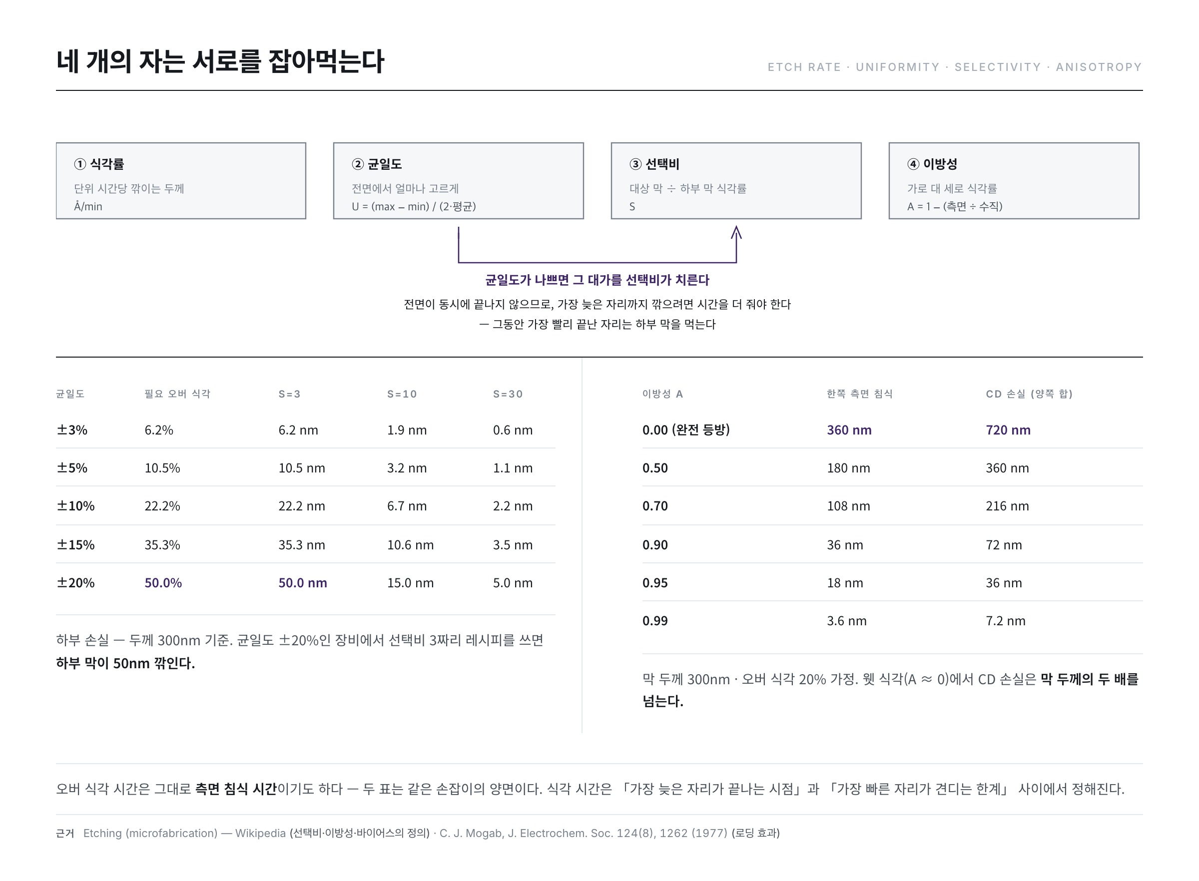
| Anisotropy A | Lateral loss per side | CD loss (both sides) |
|---|---|---|
| 0.00 (fully isotropic) | 360 nm | 720 nm |
| 0.50 | 180 nm | 360 nm |
| 0.70 | 108 nm | 216 nm |
| 0.90 | 36 nm | 72 nm |
| 0.95 | 18 nm | 36 nm |
| 0.99 | 3.6 nm | 7.2 nm |
The table was computed directly from the formula for a 300nm film with 20% over-etch. Two things to read from it. First, in wet etching (A ≈ 0) the CD loss exceeds twice the film thickness — the thicker the film the bigger the undercut, which is exactly why wet etching serves thick metal but cannot serve fine patterns. Second, raising A from 0.90 to 0.99 cuts CD loss from 72nm to 7.2nm, a factor of ten. That is why the last few percent of sidewall verticality are so expensive.
Here the earlier posts connect. The hard bake temperature of post 12 changes the PR profile, and that profile changes the path the etchant takes, which decides final CD. How strongly line-width control in anisotropic etching is entangled with mask shape was already a subject in 1979 work on polysilicon line-width control (H. A. Mayer, R. E. McConville, IEDM Technical Digest, 44 (1979)). This is why photo and etch have to be designed as one set.
The four rulers eat one another — the arithmetic of over-etch
If the four parameters were independent, you would simply optimise each. The problem is that they are interlocked, and nowhere is the interlock clearer than in over-etch.
Because the whole substrate does not finish at the same moment, there is a fastest place and a slowest place. When uniformity is ±u, the extra time needed to be sure the slowest place has cleared is
required over-etch fraction = 2u ÷ (1 − u)
Meanwhile the place that finished first is eating the underlayer. The depth cut into the underlayer is inversely proportional to selectivity S, so for a film of thickness d the underlayer loss is d · 2u ÷ ((1 − u) · S). Computed for d = 300nm:
| Uniformity | Required over-etch | Underlayer loss (S=3) | (S=10) | (S=30) |
|---|---|---|---|---|
| ±3% | 6.2% | 6.2 nm | 1.9 nm | 0.6 nm |
| ±5% | 10.5% | 10.5 nm | 3.2 nm | 1.1 nm |
| ±10% | 22.2% | 22.2 nm | 6.7 nm | 2.2 nm |
| ±15% | 35.3% | 35.3 nm | 10.6 nm | 3.5 nm |
| ±20% | 50.0% | 50.0 nm | 15.0 nm | 5.0 nm |
The message is plain: when uniformity is poor, selectivity pays the bill. On a tool with ±20% uniformity, a recipe with selectivity 3 cuts 50nm into the underlayer — and if the gate dielectric is about that thick, the device is dead. Push selectivity to 30 and the same uniformity costs only 5nm, which is survivable.
When the floor says "high selectivity lets you give generous over-etch", that is a summary of this arithmetic. And since over-etch time is also lateral-etch time, the CD table and this table are two faces of the same knob.
The loading effect — area changes the rate
The least intuitive of all the influences on etch rate is the loading effect. Same recipe, same tool — yet the rate drops when the area to be etched is large.
The reason is simple. The plasma produces a finite quantity of reactive species, and as the consuming surface grows, the share per unit area shrinks. The classic 1977 model describes this as a balance between generation and loss of reactive species, giving a curve in which etch rate falls as exposed area rises (C. J. Mogab, J. Electrochem. Soc. 124(8), 1262 (1977)). In practice it means a change of product — a change of pattern density — is a change of etch time.
Trickier still is micro-loading. Even within one substrate, narrow deep trenches etch more slowly than wide openings, because reactive species struggle to reach the bottom through a narrow mouth and products struggle to leave. This slowing with increasing aspect ratio is called RIE lag or aspect-ratio-dependent etching, and it has been organised as the dominant cause of microscopic non-uniformity (R. A. Gottscho, C. W. Jurgensen, D. J. Vitkavage, J. Vac. Sci. Technol. B 10(5), 2133 (1992); H. Jansen et al., Microelectron. Eng. 35, 45 (1997)).
The consequence is that the single number "within-substrate uniformity" hides two problems of different nature — the macroscopic distribution created by reactor geometry, and the microscopic distribution created by the pattern itself. The first is handled by the tool, the second by recipe and layout.
When to stop — endpoint detection
One of the difficulties of etching is that you cannot see whether enough has been removed. Etching for a fixed time is simplest, but a small change in film thickness or tool condition produces too much or too little.
Hence endpoint detection (EPD). As the etch reaches the underlying film, the wavelength distribution of light emitted by the plasma, or the transmittance, changes abruptly. Detecting that change is how the tool decides "it is through".
The principle lies in optical emission. Reactive species and reaction products each emit at characteristic wavelengths, so at the moment the target film disappears the emission line of its product falls while the line of the now-unconsumed reactive species rises. Judging endpoint from the intensity change of a particular emission line was already captured in patents in the late 1970s (US 4,312,732, US 4,528,438).
The tool does not stop at the endpoint signal, though. As calculated above, extra over-etch time is added to cover the slowest location. How much to give is the question — too little leaves residue, too much damages the underlayer. The signal itself has a trap as well: a small etched area gives a small signal change, so on layers with very little exposed area the transition drowns in noise.
How long does PR survive?
The last parameter is PR durability. While the etch proceeds, the PR itself is removed or deformed. Dry etching in particular attacks PR directly with ion bombardment and oxygen radicals, so the loss is heavy.
If the PR disappears first, the film beneath is exposed and the pattern collapses. PR thickness is therefore designed to "last through the etch", yet too thick a film costs resolution, so a balance is needed. The minimum thickness follows from inverting the selectivity relation — if a film of thickness d is etched by 1.2d including over-etch and the PR selectivity is S, at least 1.2d ÷ S of PR must remain.
Another point easily missed is that PR does not thin uniformly. Ions sputter more efficiently on inclined surfaces, so the PR corners erode first and a facet forms; as that corner retreats, the film beneath is exposed progressively and its sidewall tilts too. Interestingly, this PR retreat is sometimes used on purpose — the tapered profile control of post 15 is exactly that.
Two common misconceptions
- "Etching just needs enough time." The over-etch table answers this. The moment you add time, the underlayer and the sidewalls pay for it. Etch time is a narrow window between when the slowest place finishes and how long the fastest place can hold out, and the width of that window is set by uniformity and selectivity.
- "The same recipe gives the same result." The loading effect denies it. Different pattern density means a different rate; different chamber wall condition means different consumption of reactive species. A recipe is only part of the conditions.
What the floor watches — three control points
- CD and profile — is the line width within range, is the sidewall angle as designed? These two are the final indicators of etch quality.
- Residue and underlayer damage — is anything under-etched, has anything been over-etched into the layer below? These are the outcome of selectivity and over-etch design.
- Separating the levels of uniformity — you have to know whether the wobble is within-substrate, substrate-to-substrate or lot-to-lot before you can find the cause. And within a substrate, macroscopic (reactor) and microscopic (pattern) must be separated again.
In the next post (post 15) we enter the world of dry etching — how plasma turns material into gas and pumps it away, what the three generations of PE, RIE and high-density plasma each improved, and why changing one gas changes the outcome.
References
- C. J. Mogab, "The Loading Effect in Plasma Etching," J. Electrochem. Soc. 124(8), 1262 (1977) : the original description of falling etch rate with growing exposed area, via a reactive-species balance
- C. J. Mogab, A. C. Adams, D. L. Flamm, "Plasma etching of Si and SiO2 — The effect of oxygen additions to CF4 plasmas," J. Appl. Phys. 49(7), 3796 (1978) : experiment showing the etch-rate ratio between two materials can be tuned by gas composition alone
- R. A. Gottscho, C. W. Jurgensen, D. J. Vitkavage, "Microscopic uniformity in plasma etching," J. Vac. Sci. Technol. B 10(5), 2133 (1992) : review organising aspect-ratio-dependent etching (RIE lag) as a microscopic uniformity problem
- H. Jansen, M. de Boer, R. Wiegerink et al., "RIE lag in high aspect ratio trench etching of silicon," Microelectron. Eng. 35, 45 (1997) : measurement of the slowdown with increasing aspect ratio
- H. Jansen, M. de Boer, R. Legtenberg, M. Elwenspoek, "The black silicon method," J. Micromech. Microeng. 5(2), 115 (1995) : a parameter map moving etch directionality with pressure, bias and composition
- M. Surendra, C. R. Guarnieri, G. S. Selwyn, "Across wafer etch rate uniformity in a high density plasma reactor," Appl. Phys. Lett. 66(18), 2415 (1995) : measurement and modelling of the radial etch-rate distribution set by reactor geometry
- H. A. Mayer, R. E. McConville, "Linewidth control in anisotropic plasma etching of polycrystalline silicon," IEDM Technical Digest, 44 (1979) : the relation between mask shape and line-width loss in anisotropic etching
- "Loading effect and temperature dependence of etch rate of silicon materials in CF4 plasma," Microelectronics Reliability 20(6), 911 (1980) : measurement showing etch rate as a function of temperature and exposed area
- US 4,312,732 — Method for the optical monitoring of plasma discharge processing operations : judging process state by monitoring plasma emission
- US 4,528,438 — End point control in plasma etching : determining etch endpoint from the intensity change of a specific emission line
- Etching (microfabrication) — Wikipedia : definitions of selectivity, isotropy/anisotropy and bias (undercut)
- Reactive-ion etching — Wikipedia · Plasma etching — Wikipedia : the contrast between anisotropic dry and isotropic wet etching, and the basic plasma etch mechanism