Up to #05 we have followed the ways of pulling numbers out of the transfer curve. The threshold voltage, the transconductance gm, and the subthreshold slope. The subject of this installment is what was sitting inside that gm — mobility.
Mobility is different in character from the other three. The threshold voltage is a value that depends on how the device was made, but mobility is originally a property of the material. And yet, when it is measured on a device, the material's value does not come back out unchanged.
The discrepancy has two roots. The place where the current flows is not the middle of the material but the interface up against the insulator, and the resistance we measure has the resistance of the place where metal touches semiconductor mixed into it.
The condition values in the text are examples meant to show how the calculation goes, not the specifications of any particular company. Every figure quoted was checked in the open literature, and the sources are left at the end of the article.
Mobility — how fast it flows per unit of electric field
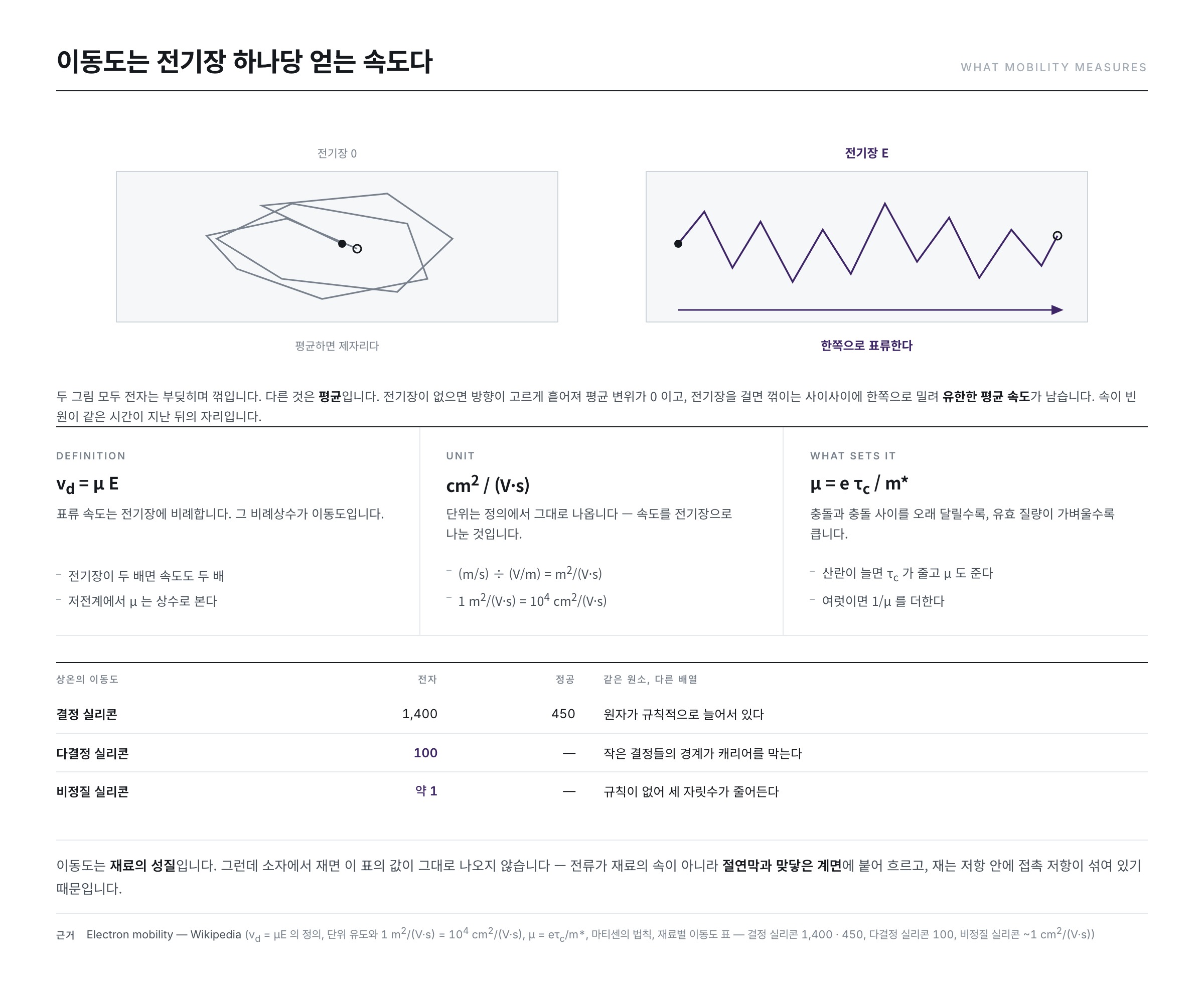
With no electric field applied, electrons wander in any direction inside the solid. The Wikipedia "Electron mobility" article writes that on average no charge is carried in any direction in that case. Apply an electric field and the electrons accelerate, but they collide again and again with crystal defects, phonons (lattice vibrations) and impurities, losing direction and energy. So instead of speeding up without limit they settle at a finite average speed, and that is the drift velocity.
Mobility is defined as the constant of proportionality joining that drift velocity to the electric field.
vd = μ E
The "Electron mobility" article writes that the unit follows immediately from this definition. The unit of velocity is m/s and the unit of electric field is V/m, so the unit of mobility is (m/s) ÷ (V/m) = m2/(V·s). In practice cm2/(V·s) is used far more often, and 1 m2/(V·s) = 104 cm2/(V·s). It looks like an unfamiliar unit, but it is nothing more than "velocity divided by electric field".
Putting numbers in gives a feel for it. Apply 1,000 V/cm to a material with μ = 10 cm2/(V·s) and vd = 10 × 1,000 = 10,000 cm/s, that is, 100 m/s.
What the expression says fixes mobility
The "Electron mobility" article derives mobility starting from Newton's second law of motion. Writing the mean time between one collision and the next as τc and the effective mass as m*,
μ = e τc / m*
The expression is itself the answer. The longer it runs without colliding (the larger τc) and the lighter the effective mass, the greater the mobility. Why mobility differs from material to material, and why electrons and holes differ even within the same material, both come out here at once.
When there are several things to collide with, they are combined by Matthiessen's rule.
1/μ = 1/μimpurity + 1/μlattice + 1/μdefect + …
Since it is a sum of reciprocals, the single smallest term drags the whole thing down. The "Electron mobility" article adds the caveat that this is an approximation and holds only when the scattering mechanisms are independent.
The values per material quoted in #01 of the earlier series also came from the table in the "Electron mobility" article — crystalline silicon at 1,400 for electrons and 450 for holes, polycrystalline silicon at 100, and amorphous silicon at about 1 cm2/(V·s). It is the same silicon, yet the more the atomic arrangement is disturbed, the more three orders of magnitude fall away.
Two ways of pulling mobility out of a device
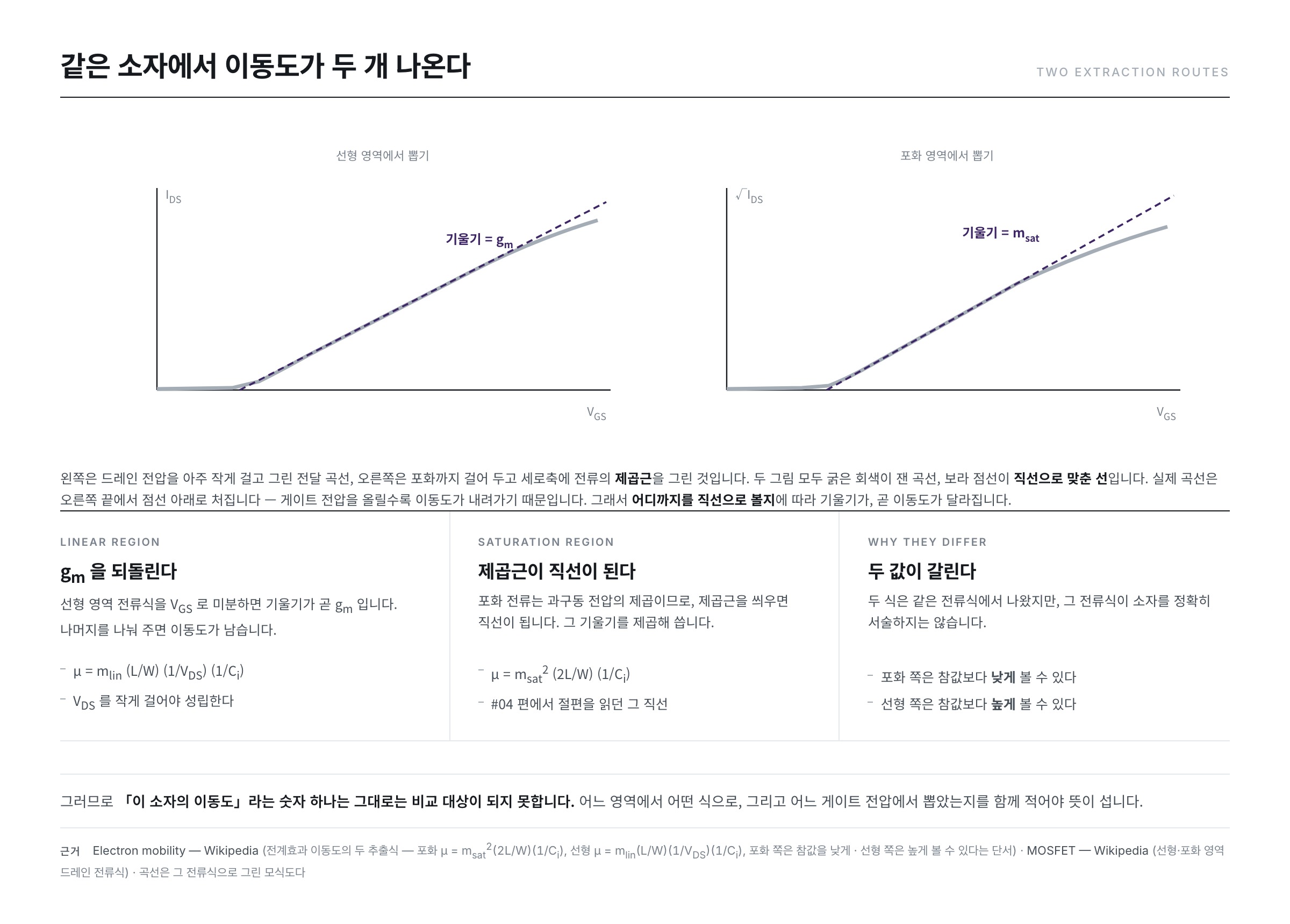
Mobility is not marked anywhere on the curve. As concluded in #03 it is a defined value, so which expression and which region it is drawn from has to be settled first. The Wikipedia "Electron mobility" article calls the mobility measured with a transistor the field-effect mobility and writes that there are two methods — the saturation region and the linear region.
This article assumes the following values in its calculations. It is the same device as in #04 — mobility μ = 10 cm2/(V·s), a gate insulator of 100 nm of silicon dioxide, and W/L = 20. Putting in the relative permittivity of silicon dioxide, 3.9, from the Wikipedia "Relative permittivity" article and the vacuum permittivity from "Vacuum permittivity" gives Cox = 3.45 × 10⁻⁸ F/cm2.
Linear region — running gm backwards
In the linear-region current expression of the Wikipedia "MOSFET" article, when VDS is very small the current is nearly a straight line in VGS, and that slope mlin is exactly the gm of #04. The "Electron mobility" article runs mobility back out of it like this.
μ = mlin × (L/W) × (1/VDS) × (1/Ci)
In #04, gm,lin for this device was 0.69 μS at VDS = 0.1 V.
μ = 0.69 × 10⁻⁶ ÷ (3.45 × 10−8 × 20 × 0.1) = 10 cm2/(V·s)
The value that went in came straight back. That is a confirmation that the expression is right, not a measurement of a device.
Saturation region — using the slope of the square root
The saturation current depends on (VGS − Vth) squared, so taking the square root of both sides gives a straight line. It is the same straight line from which the threshold voltage was read in #04, except that this time it is the slope msat that is used, not the intercept.
μ = msat2 × (2L/W) × (1/Ci)
For the same device msat = √(μCoxW / 2L) = 1.86 × 10⁻³ A1/2/V, and putting that into the expression above gives 10 cm2/(V·s) once again.
Yet in a real device the two values diverge
On paper the same value comes out. What makes them diverge is that the current expression does not describe the device exactly.
The "Electron mobility" article attaches a caveat to each of the two methods. The saturation-region method ignores channel-length modulation among other things and so can read lower than the true value, while the linear-region method, if VDS is not small enough or the gate voltage is not large enough, leaves the device outside the linear region and so can read higher than the true value.
So "the mobility of this device is such-and-such" is not complete in itself. It becomes a number that can be compared only once it carries which region and which expression it was drawn from. The conclusion of #03 repeats itself here.
Why it comes out lower than the material's value
So far the trouble has been with the expressions. Now for the physics. The Wikipedia "MOSFET" article writes that once the gate voltage passes the threshold, carriers gather in a thin layer beside the semiconductor–insulator interface and form an inversion layer. A paper on thin-film transistor models (arXiv:1812.08800) likewise starts from the premise that all of the mobile charge is confined at the interface between the semiconductor and the gate insulator.
That single sentence is the whole of the problem. The current flows not through the bulk of the material but clinging to the interface. And that interface is not smooth.
The surface roughness scattering section of the "Electron mobility" article writes, on the evidence of high-resolution electron microscopy, that the interface is not sharp at the atomic level and that the position of the boundary rises and falls by one or two atomic layers along the surface. That unevenness shakes the energy levels at the interface, and that becomes scattering. The "Electron mobility" article adds that charge trapped near the interface also acts as a scattering centre — because a defect that catches charge becomes electrically charged and pushes and pulls at the carriers passing by.
The Google patent US6548335B1 puts it more categorically — the most dominant factor causing carrier scattering in the silicon lattice is the surface roughness between the gate electrode layer and the insulating layer beneath it, that is, the silicon/silicon oxide interface, and this atomic-scale roughness increases scattering and lowers the channel carrier mobility.
Going back to Matthiessen's rule gives the conclusion immediately. A surface roughness scattering term is added to the material's mobility, so the result of summing reciprocals is necessarily smaller than the original. A mobility measured on a device coming out below the material value is not an exception but a result fixed by the structure.
Raise the gate voltage and the mobility falls
There is something more awkward still. Raising the gate voltage increases the carriers and so increases the current, but it is the same gate voltage that presses those carriers harder against the interface.
A paper analysing the mobility of 4H silicon carbide MOSFETs by the Hall effect (Materials 15, 6736, 2022) describes this process directly. As the electric field perpendicular to the interface grows, the carriers are pushed closer to the surface, and the closer they are the more surface roughness scattering comes into play, so the measured mobility falls. The Materials paper organises that decrease as a power law and reports exponents of −1.8 ± 0.2 for the n channel and −2.4 ± 0.3 for the p channel. The exponents are measured values for that material and that device, but the direction — that mobility falls as the perpendicular electric field grows — comes out of the structure in which the current flows clinging to the interface.
So the single number called "the mobility of this device" only stands up if it also says at which gate voltage it was drawn. It is the same story as the high-field mobility degradation seen in #08 of the earlier series, except that there the electric field was along the direction of flow in the channel, while here it is the field pressing the channel against the interface.
Resistance that is not the channel — contact resistance
One cause remains. The resistance measured between two terminals is not the channel's resistance alone.
The Wikipedia "Contact resistance" article defines contact resistance as the obstruction to current flow that arises because the touching surfaces do not join completely, and because of films or oxide layers on the surfaces. This resistance is present where the source and drain metal touches the semiconductor as well.
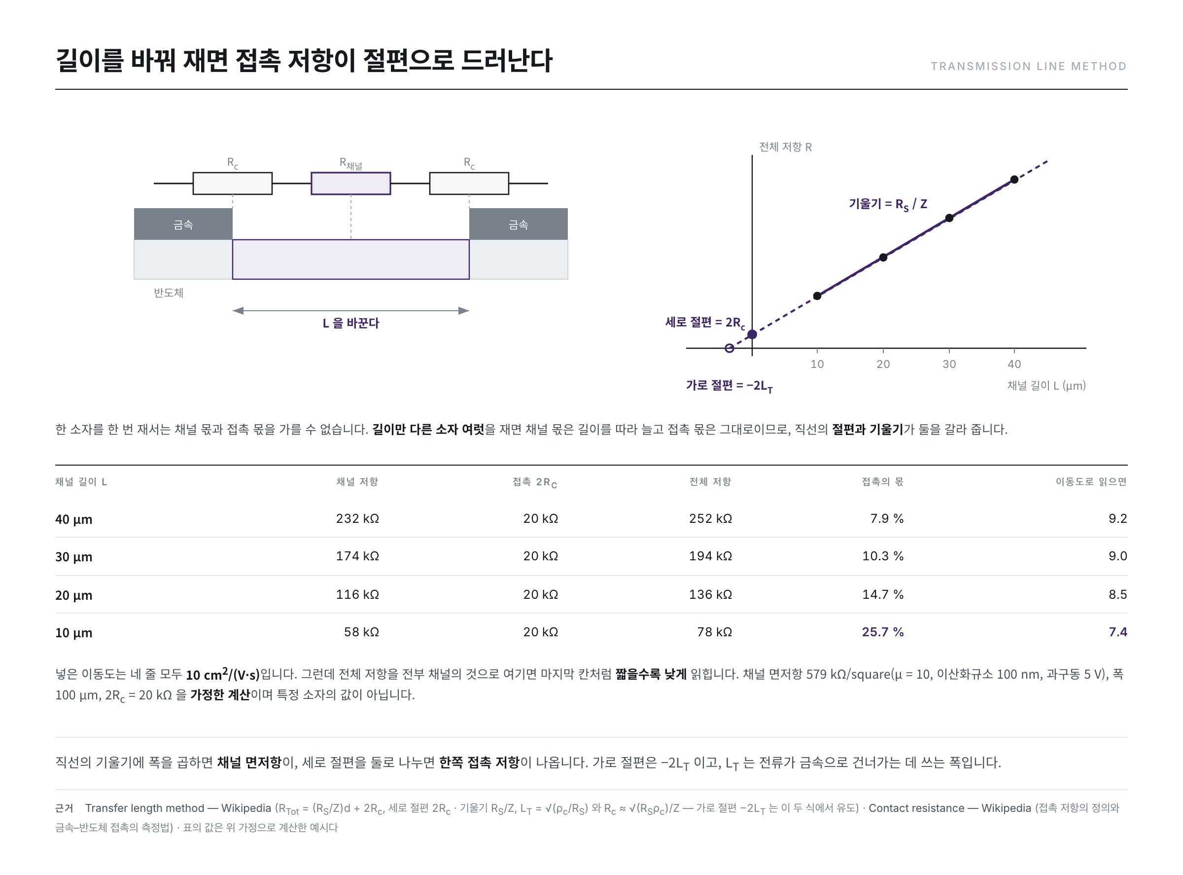
Rtotal = Rchannel + 2 Rc
There is one on the source side and one on the drain side, hence twice. But the channel resistance grows as the channel gets longer, whereas the contact resistance has nothing to do with the channel length. That is where the problem arises.
Let us count it out with the device assumed above. At an overdrive voltage of 5 V the channel sheet resistance is 1 ÷ (μ Cox VOV) = 579 kΩ/square. The channel width W is taken as 100 μm and the sum of the two contact resistances 2Rc as 20 kΩ.
- L = 40 μm — channel 232 kΩ + contact 20 kΩ = 252 kΩ. The contact's share is 7.9 %
- L = 30 μm — channel 174 kΩ + contact 20 kΩ = 194 kΩ. The contact's share is 10.3 %
- L = 20 μm — channel 116 kΩ + contact 20 kΩ = 136 kΩ. The contact's share is 14.7 %
- L = 10 μm — channel 58 kΩ + contact 20 kΩ = 78 kΩ. The contact's share is 25.7 %
Treat all of this resistance as belonging to the channel and extract a mobility, and instead of the 10 that went in only the channel's fraction comes back — 9.2 at L = 40 μm, 9.0 at 30 μm, 8.5 at 20 μm, and 7.4 at 10 μm.
Same material, same interface, and yet the shorter the channel, the lower the mobility appears to be. The mobility has not changed; only the contact resistance's share has grown.
TLM — changing the channel length and drawing a straight line
The way to separate out the contact resistance alone comes out of this. Look at the list above again and the rule appears. The total resistance is a straight line against the channel length, and extending that line to L = 0 makes the channel vanish, so what is left is nothing but the two contact resistances.
The Wikipedia "Transfer length method" article puts this into an expression.
Rtotal = (RS / Z) d + 2 Rc
RS is the sheet resistance, Z the width, and d the distance between the two contacts. The "Transfer length method" article writes that the vertical intercept is 2Rc and the slope is RS/Z. The two values that a single measurement could not separate come apart simply by measuring several times at different lengths. The thin-film transistor model paper (arXiv:1812.08800) uses the same procedure of plotting the on-resistance of devices of differing channel length against the channel length.
Drawing a straight line through the four points above gives a slope of 5.79 kΩ/μm and a vertical intercept of 20 kΩ. Half the intercept, 10 kΩ, is the resistance of one contact, and the slope multiplied by the width of 100 μm, 579 kΩ/square, is the sheet resistance of the channel. Exactly the values that went in.
The horizontal intercept has a meaning too. The "Transfer length method" article defines the length over which most of the voltage drop under the metal occurs as the transfer length LT = √(ρc / RS) and writes the contact resistance as Rc ≈ √(RS ρc) / Z. Joining the two gives Rc = RS LT / Z, and putting that into the straight-line expression above and solving for the point where Rtotal = 0 yields d = −2 LT. With the example values that is −3.45 μm, so LT is 1.73 μm. It means that this is the width the current uses to cross over into the metal.
Nor is the contact resistance a constant. arXiv:2404.19022 writes that in devices where the gate electric field modulates not only the channel but the contact resistance along with it, the established extraction methods can overestimate mobility by more than a factor of two.
Summary
- Mobility is defined by vd = μE. The unit cm2/(V·s) is "velocity divided by electric field", and μ = eτc/m* says that it is large the longer the run and the lighter the mass.
- There are two ways of drawing it out of a device. Either from gm in the linear region or from the slope of √IDS in the saturation region. The former can read high and the latter low against the true value, so the two diverge.
- The channel flows not through the bulk of the material but clinging to the insulator interface. The roughness of the interface and the charge trapped there scatter the carriers, and raising the gate voltage presses the carriers harder against the interface, so scattering increases and mobility falls.
- The measured resistance is Rchannel + 2Rc. The shorter the channel, the larger the contact's share — under the example conditions, cutting L from 40 μm to 10 μm made the mobility appear to drop from 9.2 to 7.4.
- TLM measures the total resistance while varying the channel length and draws a straight line. The vertical intercept is 2Rc, the slope is the sheet resistance divided by the width, and the horizontal intercept is −2LT.
In this installment Cox was simply a constant to be plugged in. The next one moves over to measuring that constant — a C-V measurement of capacitance rather than current, and a look at how the very interface just named as the root of the trouble shows up in the capacitance curve.
References
- Electron mobility — Wikipedia : the definition of drift velocity and vd = μE, the derivation of the unit, μ = eτc/m*, Matthiessen's rule and its caveat, surface roughness scattering (the observation that the interface rises and falls by one or two atomic layers) and scattering by trapped charge, the table of mobilities by material (crystalline silicon 1,400·450, polycrystalline silicon 100, amorphous silicon ~1), and the two extraction expressions for field-effect mobility in the linear and saturation regions with the caveat that they can read high and low against the true value
- MOSFET — Wikipedia : the statement that the inversion layer forms in a thin layer beside the semiconductor–insulator interface, the drain current expressions for the linear and saturation regions, and the definition of overdrive voltage
- Contact resistance — Wikipedia : the definition of contact resistance (incomplete joining of the touching surfaces and obstruction by surface films and oxide layers), and the statement that TLM is used as a measurement method for metal–semiconductor contacts
- Transfer length method — Wikipedia : Rtotal = (RS/Z)d + 2Rc, the vertical intercept 2Rc and slope RS/Z, the transfer length LT = √(ρc/RS) and Rc ≈ √(RSρc)/Z, and the procedure of measuring at varied spacings and fitting a straight line
- Transconductance — Wikipedia : the definition gm = ΔIout/ΔVin and the unit siemens
- Critical Evaluation of Organic Thin-Film Transistor Models (arXiv:1812.08800) : the premise that all of the mobile charge is confined at the interface between the semiconductor and the gate insulator, the statement that the resistance is divided into a channel share and a contact share, and the TLM procedure of plotting the on-resistance of devices of differing channel length against length
- Mobility and Threshold Voltage Extraction in Transistors with Gate-Voltage-Dependent Contact Resistance (arXiv:2404.19022) : the report that in devices where the gate electric field also modulates the contact resistance, the established extraction methods can overestimate mobility by more than a factor of two
- US6548335B1 — Selective epitaxy to reduce gate/gate dielectric interface roughness (Google Patents) : the statement that the most dominant factor in carrier scattering is the surface roughness between the gate electrode layer and the gate insulating layer (the silicon/silicon oxide interface), and the statement that atomic-scale roughness increases scattering and lowers the channel carrier mobility
- Study of Carrier Mobilities in 4H-SiC MOSFETs Using Hall Analysis, Materials 15, 6736 (2022) : the description that as the perpendicular electric field grows the carriers are pushed closer to the surface and surface roughness scattering increases so that the measured mobility falls, and the power-law exponents against the effective electric field of −1.8 ± 0.2 for the n channel and −2.4 ± 0.3 for the p channel
- Constants used in the calculations : Relative permittivity (silicon dioxide 3.9) · Vacuum permittivity (8.854 × 10⁻¹² F/m) — both Wikipedia
- ※ The portions quoted from Wikipedia articles in the list above are licensed under CC BY-SA 4.0.